Datasheet Summary
CY7C1161V18 CY7C1176V18 CY7C1163V18 CY7C1165V18
18-Mbit QDR™-II+ SRAM 4-Word Burst Architecture (2.5 Cycle Read Latency)
Features
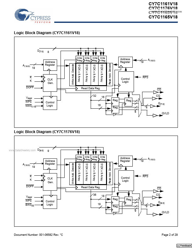
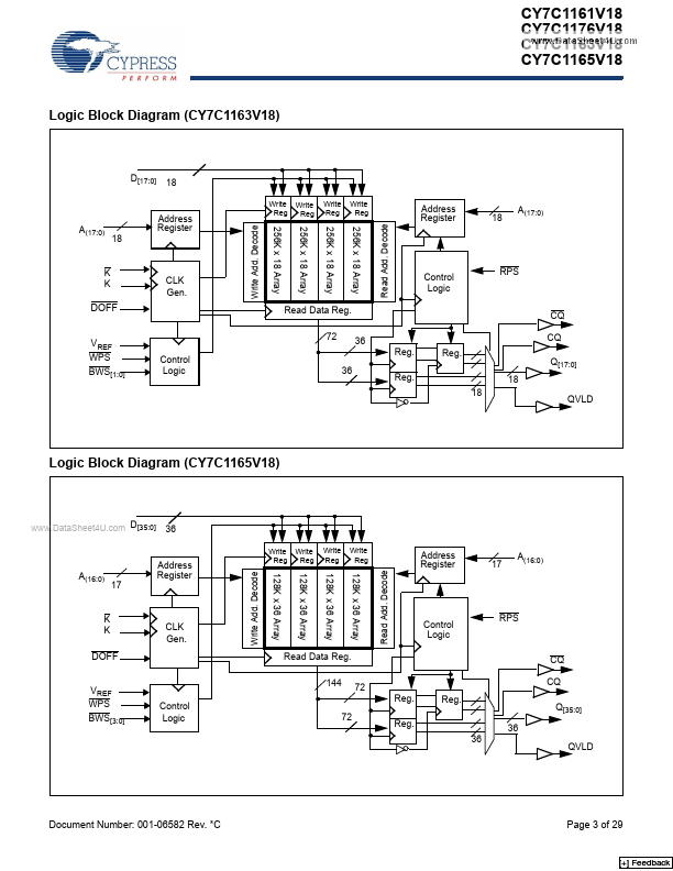
- Functional Description
The CY7C1161V18, CY7C1176V18, CY7C1163V18, and CY7C1165V18 are 1.8V Synchronous Pipelined SRAMs equipped with QDR™-II+ architecture. QDR-II+ architecture consists of two separate ports to access the memory array. The read port has dedicated data outputs to support read operations and the write port has dedicated data inputs to support write operations. QDR-II+ architecture has separate data inputs and data outputs to pletely eliminate the need to turn around the data bus that is required with mon IO devices. Each port can be...