CY7C1217F
Features
- 32K x 36 mon I/O
- 3.3V
- 5% and +10% core power supply (VDD)
- 3.3V I/O supply (VDDQ)
- Fast clock-to-output times
- 7.5 ns (117-MHz version)
- 8.0 ns (100-MHz version)
- Provide high-performance 2-1-1-1 access rate
- User-selectable burst counter supporting Pentium interleaved or linear burst sequences
- Separate processor and controller address strobes
- Synchronous self-timed write
- Asynchronous output enable
- Supports 3.3V I/O level
- Offered in JEDEC-standard 100-pin TQFP
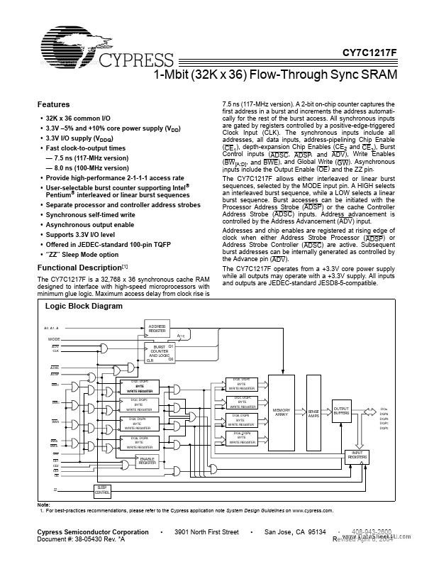
- “ZZ” Sleep Mode option Intel 7.5 ns (117-MHz version). A 2-bit on-chip counter captures the first address in a burst and increments the address automatically for the rest of the burst access. All synchronous inputs are gated by registers controlled by a positive-edge-triggered Clock Input (CLK). The synchronous inputs include all addresses, all data inputs, address-pipelining Chip Enable (CE1), depth-expansion Chip Enables (CE2 and CE3), Burst Control inputs (ADSC, ADSP, and ADV), Write Enables...