CY7C1212F
Overview
- Registered inputs and outputs for pipelined operation
- 64K × 18 common I/O architecture
- 3.3V core power supply
- 3.3V I/O operation
- Fast clock-to-output times - 3.5 ns (for 166-MHz device) - 4.0 ns (for 133-MHz device)
- Provide high-performance 3-1-1-1 access rate
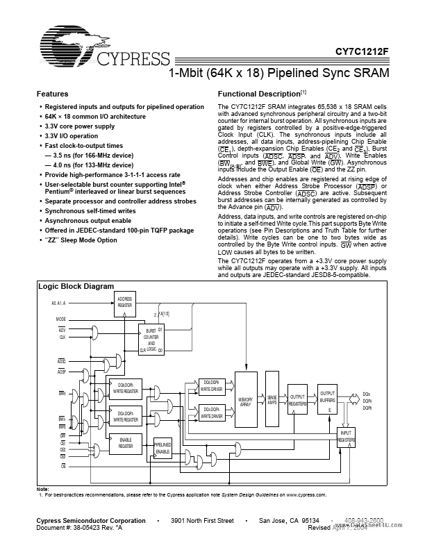
- User-selectable burst counter supporting Intel Pentium® interleaved or linear burst sequences
- Separate processor and controller address strobes
- Synchronous self-timed writes
- Asynchronous output enable


