Datasheet4U Logo Datasheet4U.com

CY7C1297F - 1-Mbit (64K x 18) Flow-Through Sync SRAM

Datasheet Summary

Description

The CY7C1297F is a 131,072 x 18 synchronous cache RAM designed to interface with high-speed microprocessors with minimum glue logic.

Features

  • 64K x 18 common I/O.
  • 3.3V.
  • 5% and +10% core power supply (VDD).
  • 3.3V I/O supply (VDDQ).
  • Fast clock-to-output times.
  • 6.5 ns (133-MHz version).
  • 7.5 ns (117-MHz version).
  • Provide high-performance 2-1-1-1 access rate.
  • User-selectable burst counter supporting Intel Pentium interleaved or linear burst sequences.
  • Separate processor and controller address strobes.
  • Synchronous self-timed write.
  • A.

📥 Download Datasheet

Datasheet preview – CY7C1297F

Datasheet Details

Part number CY7C1297F
Manufacturer Cypress Semiconductor
File Size 440.42 KB
Description 1-Mbit (64K x 18) Flow-Through Sync SRAM
Datasheet download datasheet CY7C1297F Datasheet
Additional preview pages of the CY7C1297F datasheet.
Other Datasheets by Cypress Semiconductor

Full PDF Text Transcription

Click to expand full text
CY7C1297F 1-Mbit (64K x 18) Flow-Through Sync SRAM Features • 64K x 18 common I/O • 3.3V –5% and +10% core power supply (VDD) • 3.3V I/O supply (VDDQ) • Fast clock-to-output times — 6.5 ns (133-MHz version) — 7.5 ns (117-MHz version) • Provide high-performance 2-1-1-1 access rate • User-selectable burst counter supporting Intel Pentium interleaved or linear burst sequences • Separate processor and controller address strobes • Synchronous self-timed write • Asynchronous output enable • Supports 3.3V I/O level • Offered in JEDEC-standard 100-pin TQFP • 
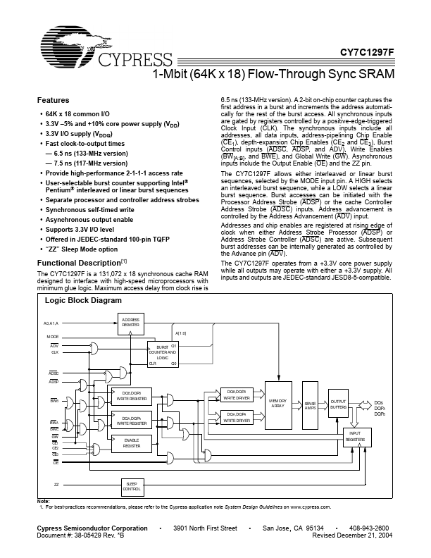
“ZZ” Sleep Mode option 6.5 ns (133-MHz version). A 2-bit on-chip counter captures the first address in a burst and increments the address automatically for the rest of the burst access.
Published: |