CY7C1351
Overview
- Pin compatible and functionally equivalent to ZBT™ devices IDT71V547, MT55L128L36F, and MCM63Z737
- Supports 66-MHz bus operations with zero wait states - Data is transferred on every clock
- Internally self-timed output buffer control to eliminate the need to use OE
- Registered inputs for Flow-Through operation
- Byte Write capability
- 128K x 36 common I/O architecture
- Single 3.3V power supply
- Fast clock-to-output times - 11.0 ns (for 66-MHz device) - 12.0 ns (for 50-MHz device) * * * *
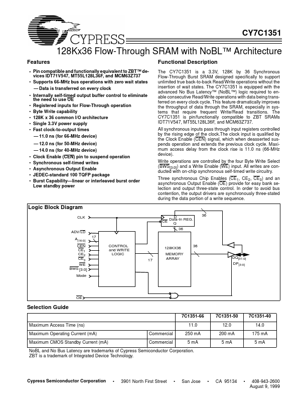
- - 14.0 ns (for 40-MHz device) Clock Enable (CEN) pin to suspend operation Synchronous self-timed writes Asynchronous Output Enable JEDEC-standard 100 TQFP package Burst Capability-linear or interleaved burst order Low standby power Functional Description The CY7C1351 is a 3.3V, 128K by 36 Synchronous Flow-Through Burst SRAM designed specifically to support unlimited true back-to-back Read/Write operations without the insertion of wait states. The CY7C1351 is equipped with the advanced No Bus Latency™ (NoBL™) logic required to enable consecutive Read/Write operations with data being transferred on every clock cycle. This feature dramatically improves the throughput of data through the SRAM, especially in systems that require frequent Write/Read transitions. The CY7C1351 is pin/functionally compatible to ZBT SRAMs IDT71V547, MT55L128L36F, and MCM63Z737. All synchronous inputs pass through input registers controlled by the rising edge of the clock input is qualified by the Clock Enable (CEN) signal, which when deasserted suspends operation and extends the previous clock cycle. Maximum access delay from the clock rise is 11.0 ns (66-MHz device). Write operations are controlled by the four Byte Write Select (BWS[3:0]) and a Write Enable (WE) input. All writes are conducted with on-chip synchronous self-timed write circuitry. Three sync