CY7C1353G
CY7C1353G is 4-Mbit (256K x 18) Flow-Through SRAM manufactured by Cypress.
Features
- Supports up to 100-MHz bus operations with zero wait states
- Data is transferred on every clock
- Pin patible and functionally equivalent to ZBT™ devices
- Internally self timed output buffer control to eliminate the need to use OE
- Registered inputs for flow-through operation
- Byte write capability
- 256K × 18 mon I/O architecture
- 2.5 V/3.3 V I/O power supply (VDDQ)
- Fast clock-to-output times
- 8.0 ns (for 100-MHz device)
- Clock enable (CEN) pin to suspend operation
- Synchronous self timed writes
- Asynchronous output enable
- Available in Pb-free 100-pin TQFP package
- Burst capability
- linear or interleaved burst order
- Low standby power
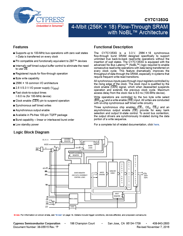
Logic Block Diagram
Functional Description
The CY7C1353G is a 3.3 V, 256K × 18 synchronous flow-through burst SRAM designed specifically to...