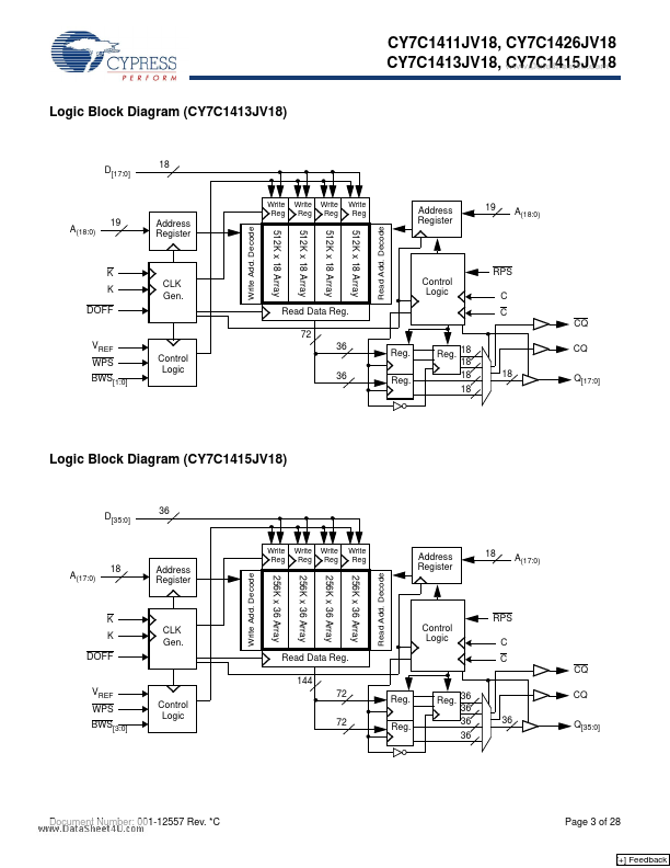
Datasheet4U Logo Datasheet4U.com

CY7C1413JV18 - (CY7C14xxJV18) 36-Mbit QDR-II SRAM 4-Word Burst Architecture

Datasheet Summary

Description

The CY7C1411JV18, CY7C1426JV18, CY7C1413JV18, and CY7C1415JV18 are 1.8V Synchronous Pipelined SRAMs, equipped with QDR™-II architecture.

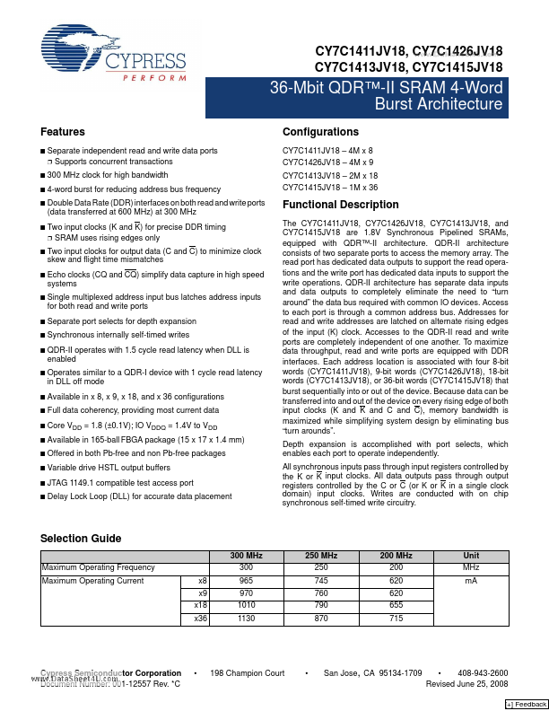
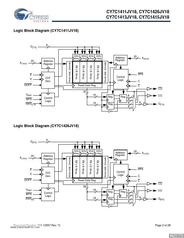
QDR-II architecture consists of two separate ports to access the memory array.

Features

  • Configurations CY7C1411JV18.
  • 4M x 8 CY7C1426JV18.
  • 4M x 9 CY7C1413JV18.
  • 2M x 18 CY7C1415JV18.
  • 1M x 36 Separate independent read and write data ports.
  • Supports concurrent transactions 300 MHz clock for high bandwidth 4-word burst for reducing address bus frequency Double Data Rate (DDR) interfaces on both read and write ports (data transferred at 600 MHz) at 300 MHz Two input clocks (K and K) for precise DDR timing.
  • SRAM uses rising edges only.

📥 Download Datasheet

Datasheet preview – CY7C1413JV18

Datasheet Details

Part number CY7C1413JV18
Manufacturer Cypress Semiconductor
File Size 723.39 KB
Description (CY7C14xxJV18) 36-Mbit QDR-II SRAM 4-Word Burst Architecture
Datasheet download datasheet CY7C1413JV18 Datasheet
Additional preview pages of the CY7C1413JV18 datasheet.
Other Datasheets by Cypress Semiconductor

Full PDF Text Transcription

Click to expand full text
CY7C1411JV18, CY7C1426JV18 www.DataSheet4U.
Published: |