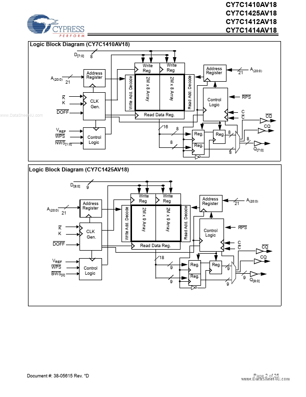
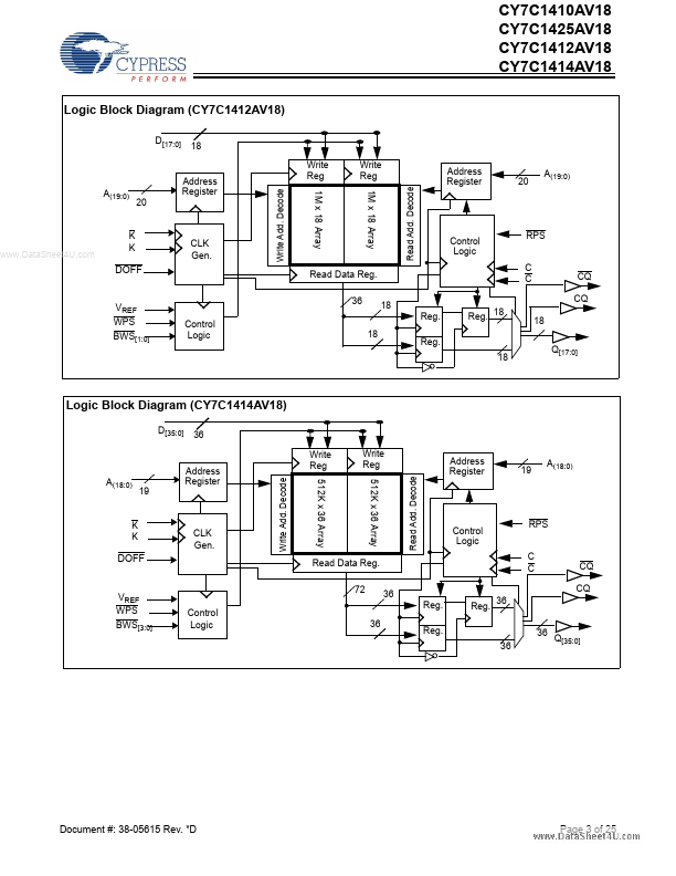
Datasheet4U Logo Datasheet4U.com

CY7C1425AV18 - 36-Mbit QDR-II SRAM 2-Word Burst Architecture

This page provides the datasheet information for the CY7C1425AV18, a member of the CY7C1412AV18 36-Mbit QDR-II SRAM 2-Word Burst Architecture family.

Datasheet Summary

Description

The CY7C1410AV18, CY7C1425AV18, CY7C1412AV18, and CY7C1414AV18 are 1.8V Synchronous Pipelined SRAMs, equipped with QDR™-II architecture.

QDR-II architecture consists of two separate ports to access the memory array.

Features

  • Separate Independent Read and Write data ports.
  • Supports concurrent transactions.
  • 250-MHz clock for high bandwidth.
  • 2-Word Burst on all accesses.
  • Double Data Rate (DDR) interfaces on both Read and Write www. DataSheet4U. com ports (data transferred at 500 MHz) @ 250 MHz.
  • Two input clocks (K and K) for precise DDR timing.
  • SRAM uses rising edges only.
  • Two input clocks for output data (C and C) to minimize clock skew and flight-.

📥 Download Datasheet

Datasheet preview – CY7C1425AV18

Datasheet Details

Part number CY7C1425AV18
Manufacturer Cypress Semiconductor
File Size 1.19 MB
Description 36-Mbit QDR-II SRAM 2-Word Burst Architecture
Datasheet download datasheet CY7C1425AV18 Datasheet
Additional preview pages of the CY7C1425AV18 datasheet.
Other Datasheets by Cypress Semiconductor

Full PDF Text Transcription

Click to expand full text
CY7C1410AV18 CY7C1425AV18 CY7C1412AV18 CY7C1414AV18 36-Mbit QDR-II™ SRAM 2-Word Burst Architecture Features • Separate Independent Read and Write data ports — Supports concurrent transactions • 250-MHz clock for high bandwidth • 2-Word Burst on all accesses • Double Data Rate (DDR) interfaces on both Read and Write www.DataSheet4U.
Published: |