Datasheet4U Logo Datasheet4U.com

CY7C1470V33 - (CY7C147xV33) 72-Mbit (2M x 36/4M x 18/1M x 72) Pipelined SRAM

General Description

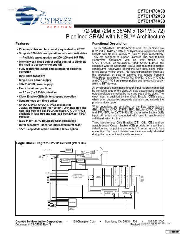
The CY7C1470V33, CY7C1472V33, and CY7C1474V33 are 3.3V, 2M x 36/4M x 18/1M x 72 Synchronous pipelined burst SRAMs with No Bus Latency™ (NoBL™) logic, respectively.

They are designed to support unlimited true back-to-back Read/Write operations with no wait states.

Key Features

  • Pin-compatible and functionally equivalent to ZBT™.
  • Supports 250-MHz bus operations with zero wait states.
  • Available speed grades are 250, 200 and 167 MHz.
  • Internally self-timed output buffer control to eliminate the need to use asynchronous OE.
  • Fully registered (inputs and outputs) for pipelined operation.
  • Byte Write capability.
  • Single 3.3V power supply.
  • 3.3V/2.5V I/O power supply.
  • Fast clock-to-output time.

📥 Download Datasheet

Full PDF Text Transcription (Reference)

The following content is an automatically extracted verbatim text from the original manufacturer datasheet and is provided for reference purposes only.

View original datasheet text
www.DataSheet4U.com CY7C1470V33 CY7C1472V33 CY7C1474V33 72-Mbit (2M x 36/4M x 18/1M x 72) Pipelined SRAM with NoBL™ Architecture Features • Pin-compatible and functionally equivalent to ZBT™ • Supports 250-MHz bus operations with zero wait states — Available speed grades are 250, 200 and 167 MHz • Internally self-timed output buffer control to eliminate the need to use asynchronous OE • Fully registered (inputs and outputs) for pipelined operation • Byte Write capability • Single 3.3V power supply • 3.3V/2.5V I/O power supply • Fast clock-to-output time — 3.0 ns (for 250-MHz device) • Clock Enable (CEN) pin to suspend operation • Synchronous self-timed writes • CY7C1470V33, CY7C1472V33 available in JEDEC-standard lead-free 100-pin TQFP, lead-free and non-lead-free 165-ball FBGA package.