CY2DP1510
CY2DP1510 is 1:10 LVPECL Fanout Buffer manufactured by Cypress.
1:10 LVPECL Fanout Buffer with Selectable Clock Input
1:10 LVPECL Fanout Buffer with Selectable Clock Input
Features
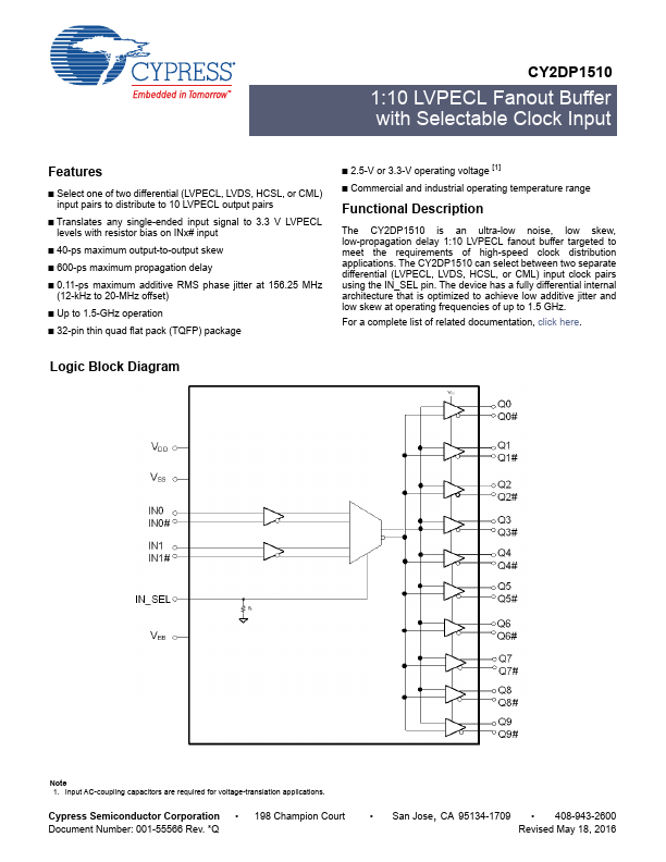
- Select one of two differential (LVPECL, LVDS, HCSL, or CML) input pairs to distribute to 10 LVPECL output pairs
- Translates any single-ended input signal to 3.3 V LVPECL levels with resistor bias on INx# input
- 40-ps maximum output-to-output skew
- 600-ps maximum propagation delay
- 0.11-ps maximum additive RMS phase jitter at 156.25 MHz
(12-k Hz to 20-MHz offset)
- Up to 1.5-GHz operation
- 32-pin thin quad flat pack (TQFP) package
- 2.5-V or 3.3-V operating voltage [1]
- mercial and industrial operating temperature range
Functional Description
The CY2DP1510 is an ultra-low noise, low skew, low-propagation delay 1:10 LVPECL fanout buffer targeted to meet the requirements of high-speed clock distribution applications. The CY2DP1510 can select between two separate differential (LVPECL, LVDS, HCSL, or CML) input clock pairs using the...