CY2DP814
CY2DP814 is 1:4 Clock Fanout Buffer manufactured by Cypress.
1:4 Clock Fanout Buffer
1:4 Clock Fanout Buffer
Features
- Low-voltage operation
- VDD = 3.3 V
- 1:4 fanout
- Single input configurable for LVDS, LVPECL, or LVTTL
- Four differential pairs of LVPECL outputs
- Drives 50-ohm load
- Low input capacitance
- Less than 4 ns typical propagation delay
- 85 ps typical output-to-output skew
- mercial temperature range
- Available in TSSOP package
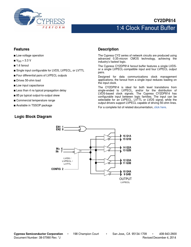
Logic Block Diagram
EN1 1 EN2 8
IN+ 6 IN- 7
LVDS / LVPECL /
LVTTL CONFIG 2
Description
The Cypress CY2 series of network circuits are produced using advanced 0.35-micron CMOS technology, achieving the industry’s fastest logic. The Cypress CY2DP814 fanout buffer Features a single LVDSor a single LVPECL-patible input and four LVPECL output pairs. Designed for data munications clock management applications, the fanout from a single input reduces loading on the input clock. The CY2DP814 is ideal for both level translations from single-ended to LVPECL, and/or for...