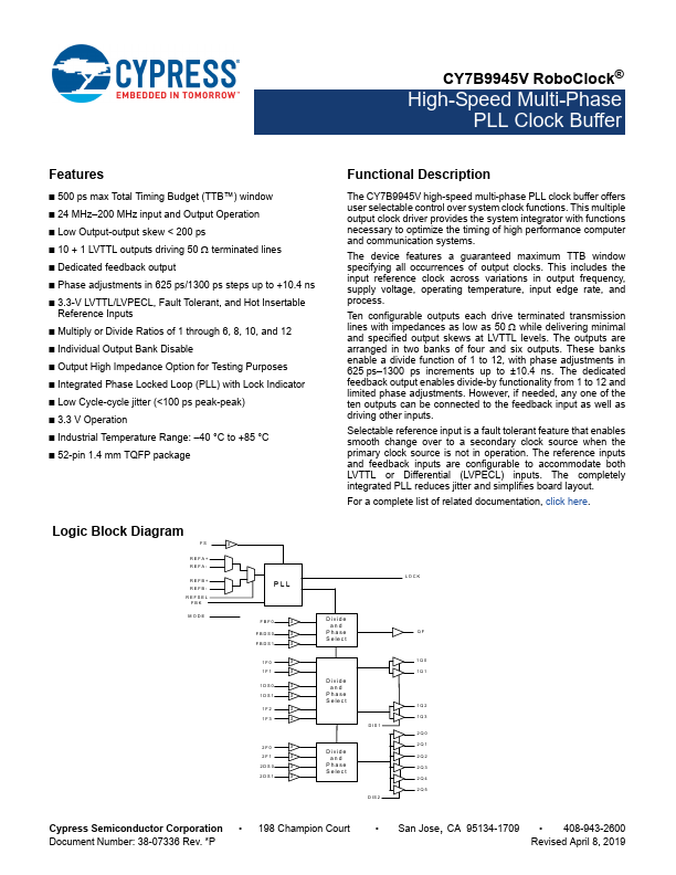
CY7B9945V Description
The CY7B9945V high-speed multi-phase PLL clock buffer offers user selectable control over system clock functions. This multiple output clock driv.
CY7B9945V Key Features
- 500 ps max Total Timing Budget (TTB™) window
- 24 MHz-200 MHz input and Output Operation
- Low Output-output skew <200 ps
- 10 + 1 LVTTL outputs driving 50 terminated lines
- Dedicated feedback output
- Phase adjustments in 625 ps/1300 ps steps up to +10.4 ns
- 3.3 V LVTTL/LVPECL, Fault Tolerant, and Hot Insertable
- Multiply or Divide Ratios of 1 through 6, 8, 10, and 12
- Individual Output Bank Disable
- Output High Impedance Option for Testing Purposes