CY7B994V Description
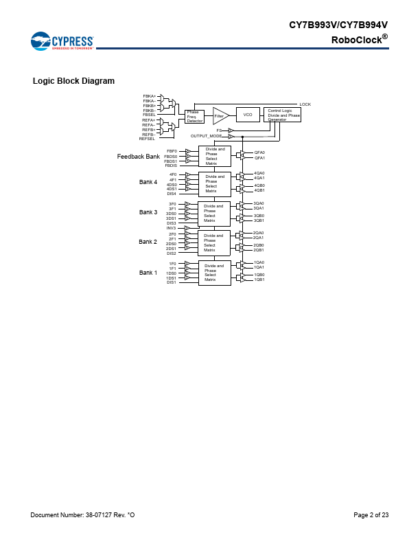
The CY7B993V and CY7B994V High-Speed Multi-Phase PLL Clock Buffers offer user-selectable control over system clock functions. This multiple-output clock driver provides the system integrator with functions necessary to optimize the timing of high-performance puter and munication systems. Eighteen configurable outputs can each drive terminated transmission lines with impedances as low as 50Ω while delivering minimal...
CY7B994V Key Features
- 12/100-MHz (CY7B993V), or 24/185-MHz (CY7B994V) output operation
- Matched pair outputs skew <200 ps
- Zero input-to-output delay
- 18 LVTTL 50% duty-cycle outputs capable of driving 50Ω terminated lines
- mercial Temp. Range with 16 outputs at 185 MHz
- Industrial Temp. Range with 6 outputs at 185 MHz
- 3.3V LVTTL/LV Differential (LVPECL), Fault Tolerant and Hot Insertable reference inputs
- Phase adjustments in 625/1300 ps steps up to ±10.4 ns
- Multiply/Divide ratios of (1-6, 8, 10, 12):(1-6, 8, 10, 12)
- Operation up to 12x input frequency