CY7C1021CV33 Description
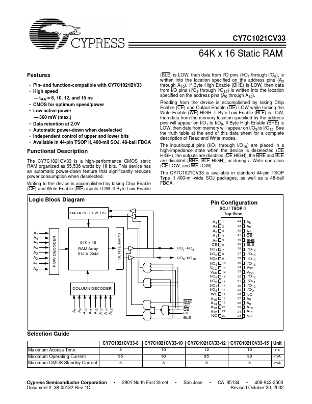
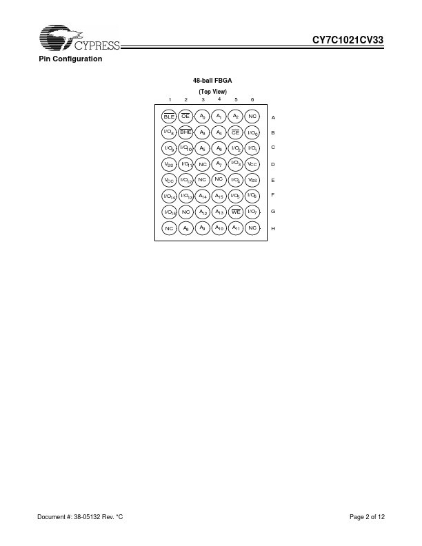
The input/output pins (I/O1 through I/O16) are placed in a high-impedance state when the device is deselected (CE HIGH), the outputs are disabled (OE HIGH), the BHE and BLE are disabled (BHE, BLE HIGH), or during a Write operation (CE LOW, and WE LOW). The CY7C1021CV33 is available in standard 44-pin TSOP Type II 400-mil-wide SOJ packages, as well as a 48-ball FBGA. Functional Description The CY7C1021CV33 is a...
CY7C1021CV33 Key Features
- Pin- and function-patible with CY7C1021BV33
- High speed
- tAA = 8, 10, 12, and 15 ns
- CMOS for optimum speed/power
- Low active power
- 360 mW (max.)
- Data retention at 2.0V
- Automatic power-down when deselected
- Independent control of upper and lower bits