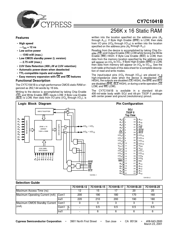
CY7C1041B Description
The input/output pins (I/O0 through I/O15) are placed in a high-impedance state when the device is deselected (CE HIGH), the outputs are disabled (OE HIGH), the BHE and BLE are disabled (BHE, BLE HIGH), or during a write operation (CE LOW, and WE LOW). The CY7C1041B is available in a standard 44-pin 400-mil-wide body width SOJ and 44-pin TSOP II package with center power and ground (revolutionary) pinout. Functional...
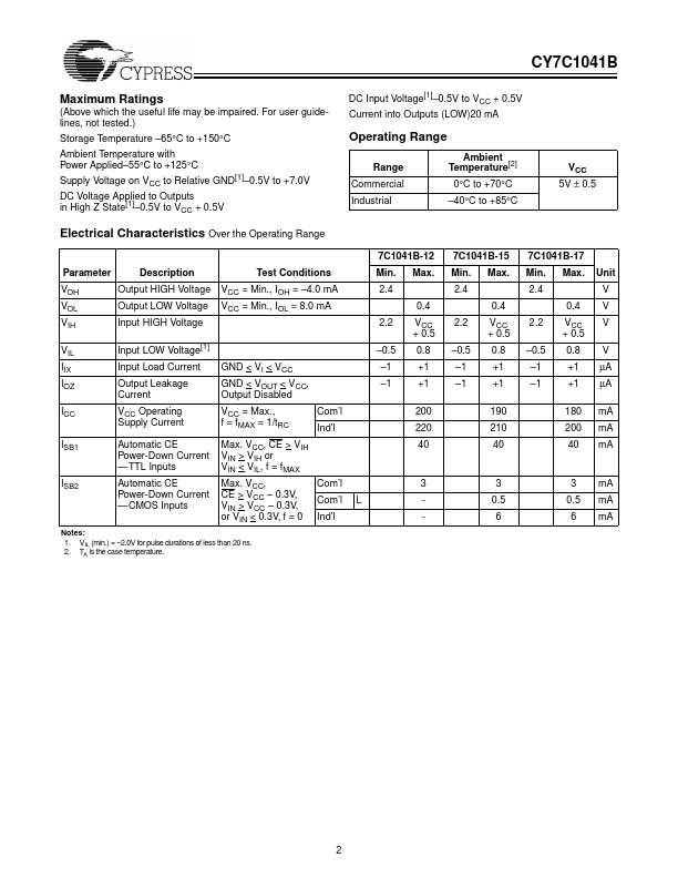
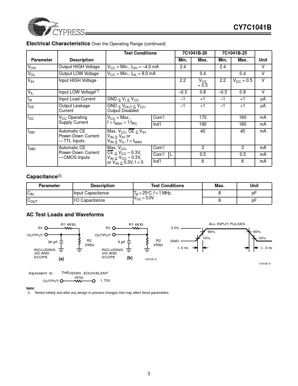
CY7C1041B Key Features
- High speed
- tAA = 12 ns
- Low active power
- 1540 mW (max.)
- Low CMOS standby power (L version)
- 2.75 mW (max.)
- 2.0V Data Retention (400 µW at 2.0V retention)
- Automatic power-down when deselected
- TTL-patible inputs and outputs