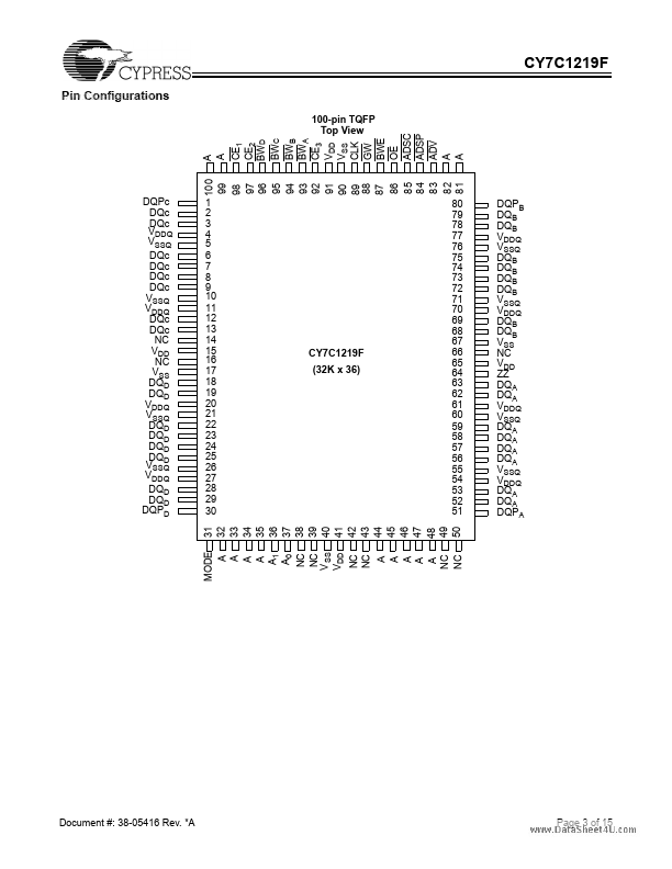
CY7C1219F Description
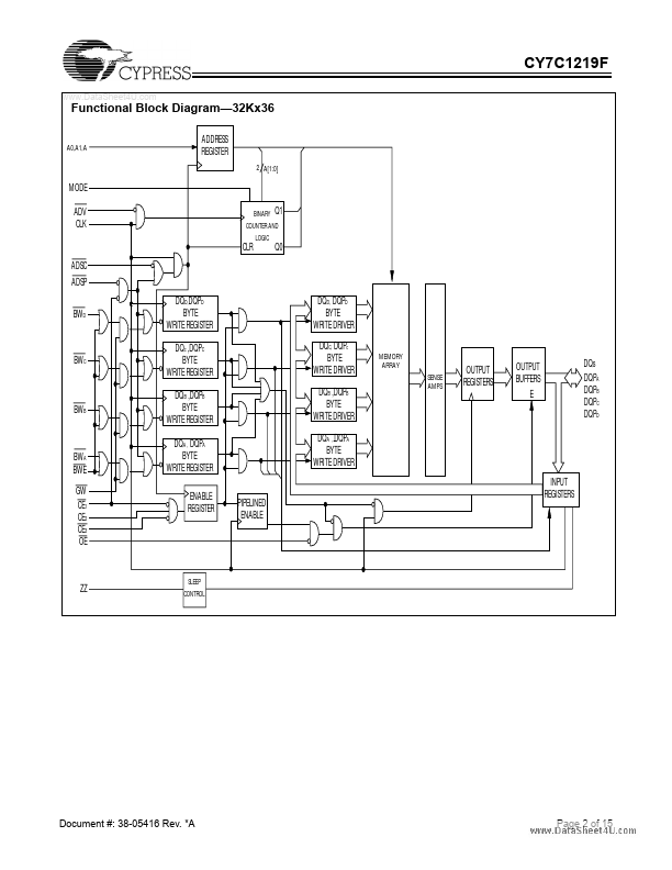
[1] The CY7C1219F SRAM integrates 32,768 x 36 SRAM cells with advanced synchronous peripheral circuitry and a two-bit counter for internal burst operation. All synchronous inputs are gated by registers controlled by a positive-edge-triggered Clock Input (CLK). The synchronous inputs include all addresses, all data inputs, address-pipelining Chip Enable (CE1), depth-expansion Chip Enables (CE2 and CE3), Burst Control...
CY7C1219F Key Features
- Registered inputs and outputs for pipelined operation
- Optimal for performance (Double-Cycle deselect)
- Depth expansion without wait state
- 32K × 36-bit mon I/O architecture
- 3.3V -5% and +10% core power supply (VDD)
- 3.3V I/O supply (VDDQ)
- Fast clock-to-output times
- 3.5 ns (for 166-MHz device)
- 4.0 ns (for 133-MHz device)
- Provide high-performance 3-1-1-1 access rate