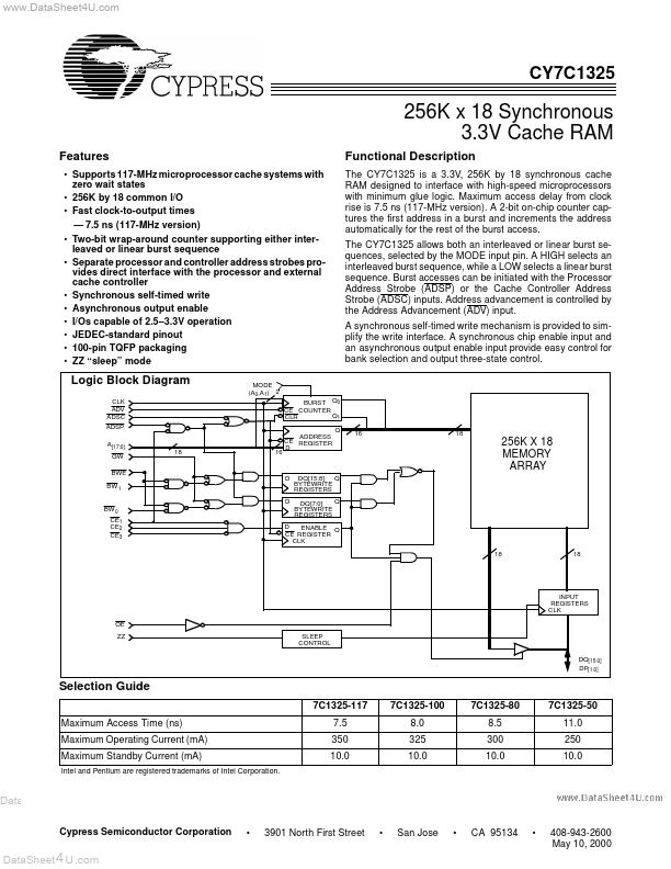
CY7C1325 Description
The CY7C1325 is a 3.3V, 256K by 18 synchronous cache RAM designed to interface with high-speed microprocessors with minimum glue logic. Maximum access delay from clock rise is 7.5 ns (117-MHz version). A 2-bit on-chip counter captures the first address in a burst and increments the address automatically for the rest of the burst access.
CY7C1325 Key Features
- Supports 117-MHz microprocessor cache systems with zero wait states
- 256K by 18 mon I/O
- Fast clock-to-output times
- 7.5 ns (117-MHz version)
- Two-bit wrap-around counter supporting either interleaved or linear burst sequence
- Separate processor and controller address strobes provides direct interface with the processor and external cache contro
- Synchronous self-timed write
- Asynchronous output enable
- I/Os capable of 2.5-3.3V operation
- JEDEC-standard pinout