CY7C1325G
Features
- 256K × 18 mon I/O
- 3.3 V core power supply (VDD)
- 2.5 V or 3.3 V I/O power supply (VDDQ)
- Fast clock-to-output times
- 6.5 ns (133 MHz version)
- Provide high performance 2-1-1-1 access rate
- User selectable burst counter supporting Intel Pentium interleaved or linear burst sequences
- Separate processor and controller address strobes
- Synchronous self timed write
- Asynchronous output enable
- Available in Pb-free 100-pin TQFP package
- “ZZ” sleep mode option
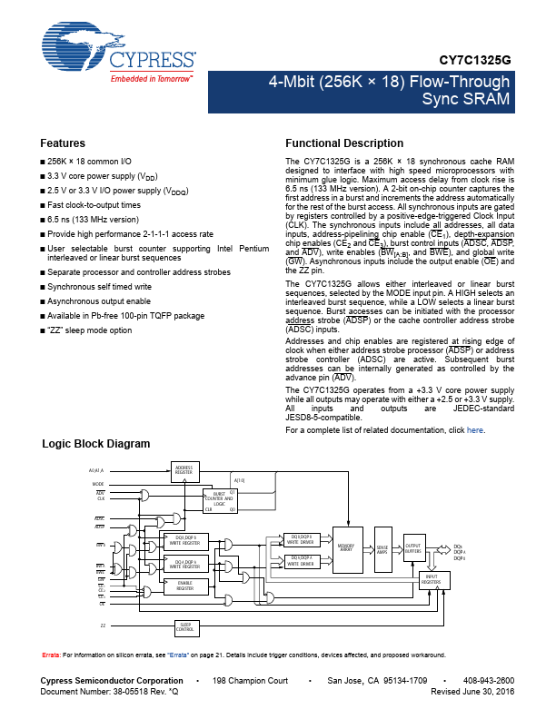
Logic Block Diagram
Functional Description
The CY7C1325G is a 256K × 18 synchronous cache RAM designed to interface with high speed microprocessors with minimum glue logic. Maximum access delay from clock rise is 6.5 ns (133 MHz version). A 2-bit on-chip counter captures the first address in a burst and increments the address automatically for the rest of the burst access. All...