EDI8L21664V
EDI8L21664V is External SRAM Memory Solution manufactured by EDI.
Features
DSP Memory Solution
- Texas Instruments TMS320C54x 3.3V Operating Supply Voltage Access Times of 10, 12 and 15ns Single Write Control and Output Enable Lines One Chip Enable Line per Memory Bank 50% Space Savings vs. Monolithic TSOPs Upgrade Path Available in Same Footprint Multiple VCC and VSS Pins Reduced Inductance and Capacitance 74 pin BGA, JEDEC MO-151 The EDI8L21664Vxx BC is a 3.3V, 2x64Kx16 SRAM constructed with two 64Kx16 die mounted on a multilayer laminate substrate. The device is packaged in a 74 lead, 15mm by 15mm, BGA. Operating with a 3.3V power supply and with access times as fast as 10ns, the device allows the user to develop a fast external memory for Texas Instuments' TMS320C54x DSP. The device consists of two separate banks of 64Kx16 of memory. Each bank has a separate Chip Enable pin and higher order address select pin. Bank 'A' is controlled using CE1 and A15A. Bank 'B' is controlled using CE2 and A15B. The two banks have mon I/Os (DQ0-15) and control lines (WE and G).
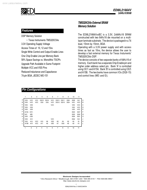
Pin Configurations
1 A B C D E F G H J K L VSS VSS VSS VSS VSS A15A N/C VSS VSS VSS A15B 1 2 VCC VCC VSS VSS VSS CE1 WE CE2 A14 A12 A13 2 3 VCC VCC 4 5 6 VCC VCC VCC 7 8 9 DQ9 DQ4 10 DQ8 VCC VSS VSS VSS DQ3 DQ5 DQ6 DQ2 A0 A3 10 11 N/C VCC VCC VCC VCC DQ7 DQ0 DQ1 NC G A1 11 A B C D E F G H J K L
DQ15 DQ14 VSS VSS
DQ13 DQ11 DQ12 DQ10
VCC VCC 3
A10 A11 4
A8 A9 5
VCC VSS VSS 6
A6 A7 7
A4 VSS 8
A2 A5 9
Electronic Designs Incorporated
- One Research Drive
- Westborough, MA 01581 USA
- 508-366-5151
- FAX 508-836-4850
- http://.electronic-designs. 1 EDI8L21664V Rev. 0 1/98 ECO #9704
Block Diagram
A0-A14 G WE CE1 A15 A
64K x 16 SRAM
DQ0-DQ15
CE2 A15 B
64K x 16 SRAM
Pin Descriptions
Pin Symbol A0-A14 A15A A15B WE CE1 CE2 G DQ0-15 Vcc Vss Type Input Input Input Input Input Input Input Input/Output Supply Ground Description
Addresses Addresses: A15 on Bank 'A' of memory Addresses: A15 on Bank 'B' of memory Write Enable: This active LOW input allows a full 16-bit...