M12L16161A-7TG2R
M12L16161A-7TG2R is 512K x 16Bit x 2Banks Synchronous DRAM manufactured by Elite Semiconductor Microelectronics Technology.
- Part of the M12L16161A-2R comparator family.
- Part of the M12L16161A-2R comparator family.
ESMT
SDRAM
M12L16161A (2R)
512K x 16Bit x 2Banks Synchronous DRAM
Features
GENERAL DESCRIPTION
- JEDEC standard 3.3V power supply
- LVTTL patible with multiplexed address
- Dual banks operation
- MRS cycle with address key programs
- CAS Latency (2 & 3 )
- Burst Length (1, 2, 4, 8 & full page)
- Burst Type (Sequential & Interleave)
- All inputs are sampled at the positive going edge of the system clock
The M12L16161A is 16,777,216 bits synchronous high data rate Dynamic RAM organized as 2 x 524,288 words by 16 bits, fabricated with high performance CMOS technology. Synchronous design allows precise cycle control with the use of system clock I/O transactions are possible on every clock cycle. Range of operating frequencies, programmable burst length and programmable latencies allow the same device to be useful for a variety of high bandwidth, high performance memory system applications.
- Burst Read Single-bit Write operation
- DQM for masking
ORDERING INFORMATION
- Auto & self refresh
- 32ms refresh period (2K cycle)
Product ID
Max Freq. Package ments
M12L16161A-5TG2R M12L16161A-7TG2R
200MHz 143MHz
TSOP(II) TSOP(II)
Pb-free Pb-free
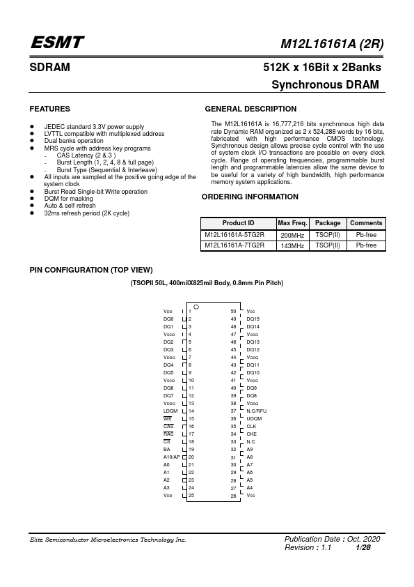
PIN CONFIGURATION (TOP VIEW)
(TSOPII 50L, 400mil X825mil Body, 0.8mm Pin...