M12L2561616A-5TG2S
M12L2561616A-5TG2S is 4M x 16 Bit x 4 Banks Synchronous DRAM manufactured by Elite Semiconductor Microelectronics Technology.
ESMT
SDRAM
M12L2561616A (2S)
4M x 16 Bit x 4 Banks Synchronous DRAM
Features y JEDEC standard 3.3V power supply y LVTTL patible with multiplexed address y Four banks operation y MRS cycle with address key programs
- CAS Latency ( 2 & 3 )
- Burst Length ( 1, 2, 4, 8 & full page )
- Burst Type ( Sequential & Interleave ) y All inputs are sampled at the positive going edge of the system clock y Burst Read single write operation y DQM for masking y Auto & self refresh y 64ms refresh period (8K cycle) y All Pb-free products are Ro HS-pliant
ORDERING INFORMATION
Product ID M12L2561616A-5TG2S M12L2561616A-6TG2S M12L2561616A-7TG2S M12L2561616A-5BG2S M12L2561616A-6BG2S M12L2561616A-7BG2S
Max Freq. Package ments
200MHz TSOP II Pb-free
166MHz TSOP II Pb-free
143MHz TSOP II Pb-free
200MHz BGA
Pb-free
166MHz BGA
Pb-free
143MHz BGA
Pb-free
GENERAL DESCRIPTION
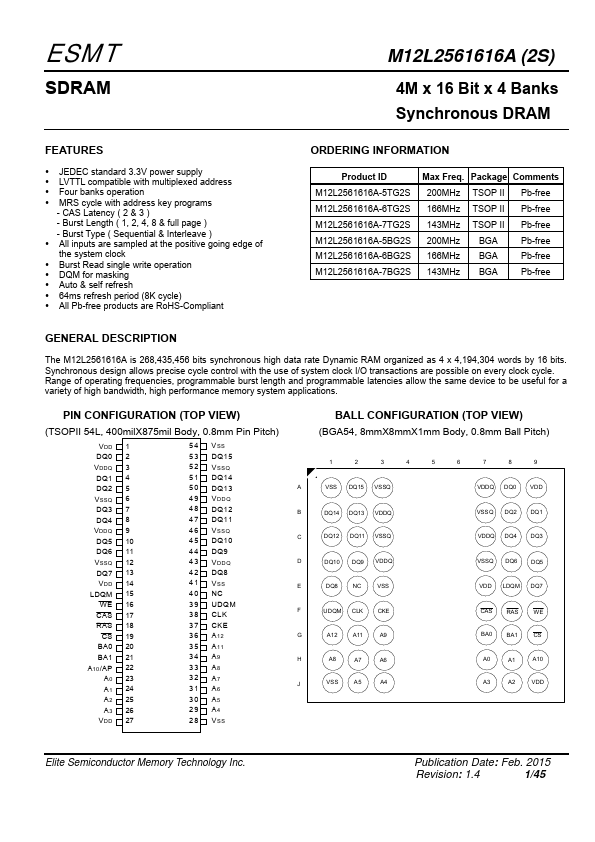
The M12L2561616A is 268,435,456 bits synchronous high data rate Dynamic RAM organized as 4 x 4,194,304 words by 16 bits. Synchronous design allows precise cycle control with the use of system clock I/O transactions are possible on every clock cycle. Range of operating frequencies, programmable burst length and programmable latencies allow the same device to be useful for a variety of high bandwidth, high performance memory system applications.
PIN CONFIGURATION (TOP VIEW)
(TSOPII 54L, 400mil X875mil Body, 0.8mm Pin Pitch)
VDD 1 DQ0 2 VDDQ 3 DQ1 4 DQ2 5 VSSQ 6 DQ3 7 DQ4 8 VDDQ 9 DQ5 10 DQ6 11 VSSQ 12 DQ7 13 VDD 14 LDQM 15 WE 16 CAS 17 RAS 18
CS 19 BA0 20 BA1 21 A10/AP 22
A0 23 A1 24 A2 25 A3 26 VDD 27
54 VSS 53 DQ15 52 VSSQ 51 DQ14 50 DQ13 49 VDDQ 48 DQ12 47 DQ11 46 VSSQ 45 DQ10 44 DQ9 43 VDDQ 42 DQ8 41 VSS 40 NC 39 UDQM 38 CLK 37 CKE 36 A12 35 A11 34 A9 33 A8 32 A7 31 A6 30 A5 29 A4 28 VSS
BALL CONFIGURATION (TOP VIEW) (BGA54, 8mm X8mm X1mm Body, 0.8mm Ball Pitch)
VSS DQ15...