M14D128168A-1.5BG2Y Description
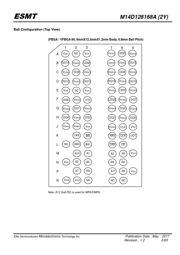
Pin Name A0~A12, BA0,BA1 DQ0~DQ15 RAS CAS WE VSS VDD DQS, DQS (LDQS, LDQS UDQS, UDQS ) ODT NC Function Address inputs - Row address A0~A11 - Column address A0~A8 A12: use for MRS/EMRS.
M14D128168A-1.5BG2Y Key Features
- JEDEC Standard
- VDD = 1.8V ± 0.1V, VDDQ = 1.8V ± 0.1V
- Internal pipelined double-data-rate architecture; two data access per clock cycle
- Bi-directional differential data strobe (DQS, DQS ); DQS can be disabled for single-ended data strobe operation
- On-chip DLL
- Differential clock inputs (CLK and CLK )
- DLL aligns DQ and DQS transition with CLK transition
- 1KB page size
- Row address: A0 to A11
- Column address: A0 to A8