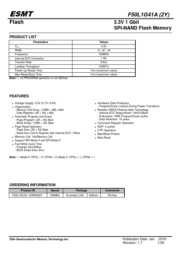
F50L1G41A
Description
The serial electrical interface follows the industry-standard serial peripheral interface (SPI), providing a cost-effective non-volatile memory storage solution in systems where pin count must be kept to a minimum. The device is a 1Gb SLC SPI-NAND Flash memory device based on the standard parallel NAND Flash, but new command protocols and registers are defined for SPI operation.
Key Features
- Mode 0: CPOL = 0, CPHA = 0; Mode 3: CPOL = 1, CPHA = 1


