EDD2516AETA
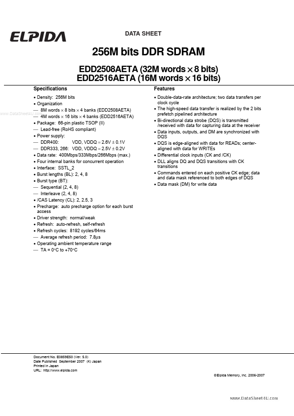
EDD2516AETA is 256M bits DDR SDRAM manufactured by Elpida Memory.
- Part of the EDD2508AETA comparator family.
- Part of the EDD2508AETA comparator family.
Features
- Double-data-rate architecture; two data transfers per clock cycle
- The high-speed data transfer is realized by the 2 bits prefetch pipelined architecture
- Bi-directional data strobe (DQS) is transmitted /received with data for capturing data at the receiver
- Data inputs, outputs, and DM are synchronized with DQS
- DQS is edge-aligned with data for READs; centeraligned with data for WRITEs
- Differential clock inputs (CK and /CK)
- DLL aligns DQ and DQS transitions with CK transitions
- mands entered on each positive CK edge; data and data mask referenced to both edges of DQS
- Data mask (DM) for write data
Document No. E0859E50 (Ver. 5.0) Date Published September 2007 (K) Japan Printed in Japan URL: http://.elpida. Elpida Memory, Inc. 2006-2007
EDD2508AETA, EDD2516AETA
Ordering Information
Part number EDD2508AETA-5B-E EDD2508AETA-5C-E EDD2508AETA-6B-E EDD2508AETA-7A-E EDD2508AETA-7B-E EDD2516AETA-5B-E EDD2516AETA-5C-E EDD2516AETA-6B-E EDD2516AETA-7A-E EDD2516AETA-7B-E Mask version E Organization (words × bits) 32M × 8 Internal banks 4 Data rate Mbps (max.) 400 333 266 16M × 16 400 333 266 JEDEC speed bin (CL-t RCD-t RP) DDR400B (3-3-3) DDR400C (3-4-4) DDR333B (2.5-3-3) DDR266A (2-3-3) DDR266B (2.5-3-3) DDR400B (3-3-3) DDR400C (3-4-4) DDR333B (2.5-3-3) DDR266A (2-3-3) DDR266B (2.5-3-3) Package 66-pin Plastic TSOP (II)
..
Part Number
E D D 25 08 A E TA
- 5B
- E
Elpida Memory
Type D: Monolithic Device
Product Family D: DDR SDRAM
Environment Code E: Lead Free (Ro HS pliant) Speed 5B: DDR400B (3-3-3) 5C: DDR400C (3-4-4) 6B: DDR333B (2.5-3-3) 7A: DDR266A (2-3-3) 7B: DDR266B (2.5-3-3) Package TA: TSOP (II)
Density / Bank 25: 256M / 4-bank Organization 08: x8 16: x16 Power Supply, Interface A: 2.5V, SSTL_2 Die Rev.
Speed Grade patibility
Operating Frequencies Speed bin DDR400B DDR400C DDR333B DDR266A DDR266B CL2 133MHz 133MHz 133MHz 133MHz 100MHz CL2.5 166MHz 166MHz 166MHz 133MHz 133MHz CL3 200MHz 200MHz 166MHz 133MHz 133MHz
Data Sheet E0859E50 (Ver....


