Datasheet4U Logo Datasheet4U.com

EM6AA320 - 8M x 32 DDR SDRAM

Description

Table 1.

Pin Details of EM6AA320 Description Differential Clock: CK, CK# are driven by the system clock.

All SDRAM input commands are sampled on the positive edge of CK.

Features

  • Fast clock rate: 300/275/250/200 MHz.
  • Differential Clock CK & CK# input.
  • 4 Bi-directional DQS. Data transactions on both edges of DQS (1DQS / Byte).
  • DLL aligns DQ and DQS transitions.
  • Edge aligned data & DQS output.
  • Center aligned data & DQS input.
  • 4 banks operation.
  • Programmable mode and extended mode registers - CAS# Latency: 3, 4, 5 - Burst length: 2, 4, 8 - Burst Type: Sequential & Interleave.
  • Full page burst l.

📥 Download Datasheet

Datasheet preview – EM6AA320

Datasheet Details

Part number EM6AA320
Manufacturer Etron Technology
File Size 369.04 KB
Description 8M x 32 DDR SDRAM
Datasheet download datasheet EM6AA320 Datasheet
Additional preview pages of the EM6AA320 datasheet.
Other Datasheets by Etron Technology

Full PDF Text Transcription

Click to expand full text
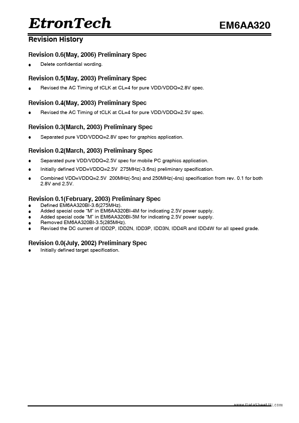
EtronTech Revision History Revision 0.6(May, 2006) Preliminary Spec Delete confidential wording. EM6AA320 Revision 0.5(May, 2003) Preliminary Spec Revised the AC Timing of tCLK at CL=4 for pure VDD/VDDQ=2.8V spec. Revision 0.4(May, 2003) Preliminary Spec Revised the AC Timing of tCLK at CL=4 for pure VDD/VDDQ=2.5V spec. Revision 0.3(March, 2003) Preliminary Spec Separated pure VDD/VDDQ=2.8V spec for graphics application. Revision 0.2(March, 2003) Preliminary Spec Separated pure VDD/VDDQ=2.5V spec for mobile PC graphics application. Initially defined VDD=VDDQ=2.5V 275MHz(-3.6ns) preliminary specification. Combined VDD=VDDQ=2.5V 200MHz(-5ns) and 250MHz(-4ns) specification from rev. 0.1 for both 2.8V and 2.5V. Revision 0.1(February, 2003) Preliminary Spec Defined EM6AA320BI-3.6(275MHz).
Published: |