FLK027XP
FLK027XP is GaAs FET & HEMT Chips manufactured by Eudyna Devices.
FLK027XP, FLK027XV
GaAs FET & HEMT Chips Features
- -
- - High Output Power: P1dB = 24.0dBm(Typ.) High Gain: G1dB = 7.0dB(Typ.) High PAE: ηadd = 32%(Typ.) Proven Reliability
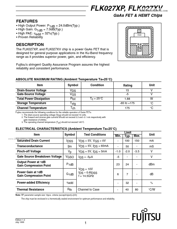
Source Gate
Drain
DESCRIPTION
The FLK027XP, and FLK027XV chip is a power GaAs FET that is designed for general purpose applications in the Ku-Band frequency range as it provides superior power, gain, and efficiency. Fujitsu’s stringent Quality Assurance Program assures the highest reliability and consistent performance....