EMB06K03HP
EMB06K03HP is N-Channel Logic Level Enhancement Mode Field Effect Transistor manufactured by Excelliance MOS.
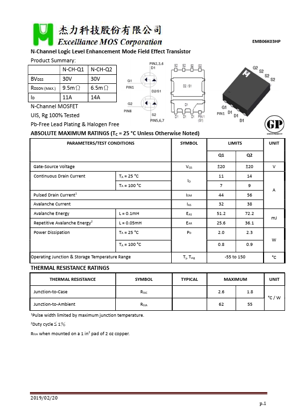
N-Channel Logic Level Enhancement Mode Field Effect Transistor
Product Summary:
N-CH-Q1 N-CH-Q2
BVDSS
30V
30V
RDSON (MAX.) 9.5mΩ 6.5mΩ
11A
14A
N-Channel MOSFET
UIS, Rg 100% Tested
Pb-Free Lead Plating & Halogen Free
ABSOLUTE MAXIMUM RATINGS (TC = 25 °C Unless Otherwise Noted)
PARAMETERS/TEST CONDITIONS
SYMBOL
Gate-Source Voltage Continuous Drain Current
Pulsed Drain Current1 Avalanche Current Avalanche Energy Repetitive Avalanche Energy2 Power Dissipation
TA = 25 °C TA = 100 °C
L = 0.1m H L = 0.05m H TA = 25 °C
TA = 100 °C
Operating Junction & Storage Temperature Range
THERMAL RESISTANCE RATINGS
THERMAL RESISTANCE
SYMBOL
Junction-to-Case
RJC
Junction-to-Ambient
RJA
1Pulse width limited by maximum junction temperature. 2Duty cycle 1% RJA when mounted on a 1 in2 pad of 2 oz copper.
VGS ID IDM IAS EAS EAR PD
Tj, Tstg
TYPICAL
LIMITS
Q1
Q2
±20
±20...