EMD04N10E
EMD04N10E is Single N-Channel Logic Level Enhancement Mode Field Effect Transistor manufactured by Excelliance MOS.
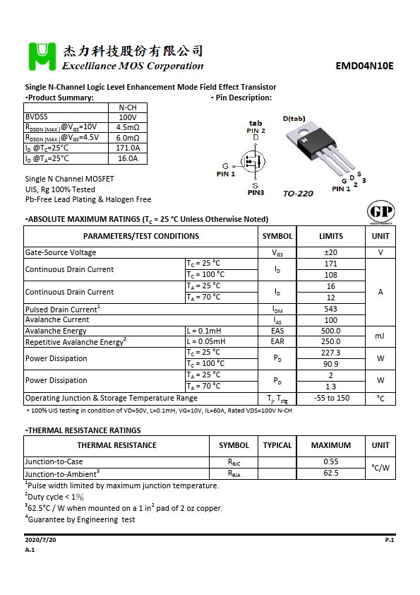
Description
:
N-CH
BVDSS
100V
RDSON (MAX.)@VGS=10V RDSON (MAX.)@VGS=4.5V
4.5mΩ 6.0mΩ
ID @TC=25℃
171.0A
ID @TA=25℃
16.0A
Single N Channel MOSFET UIS, Rg 100% Tested Pb-Free Lead Plating & Halogen Free
- ABSOLUTE MAXIMUM RATINGS (TC = 25 °C Unless Otherwise Noted)
PARAMETERS/TEST CONDITIONS
SYMBOL
Gate-Source Voltage Continuous Drain Current
TC = 25 °C TC = 100 °C
Continuous Drain Current Pulsed Drain Current1
TA = 25 °C TA = 70 °C
Avalanche Current
Avalanche Energy Repetitive Avalanche Energy2
L = 0.1m H
L = 0.05m H
Power Dissipation
TC = 25 °C TC = 100 °C
Power Dissipation
TA = 25 °C TA = 70 °C
Operating Junction & Storage Temperature Range
Tj, Tstg
- 100% UIS testing in condition of VD=50V, L=0.1m H, VG=10V, IL=60A, Rated VDS=100V N-CH
- THERMAL RESISTANCE...