EMF16P01VAT
EMF16P01VAT is MOSFET manufactured by Excelliance MOS.
P‐Channel Logic Level Enhancement Mode Field Effect Transistor
Product Summary:
BVDSS
‐10V
RDSON (MAX.)
16mΩ
ID
‐10A
S
Pb‐Free Lead Plating & Halogen Free
ABSOLUTE MAXIMUM RATINGS (TA = 25 °C Unless Otherwise Noted)
PARAMETERS/TEST CONDITIONS
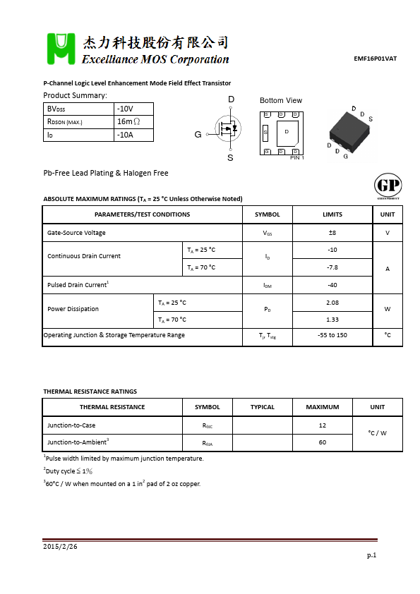
Bottom View
S DD
GD D
PIN 1
SYMBOL
LIMITS
UNIT
Gate‐Source Voltage
Continuous Drain Current Pulsed Drain Current1
TA = 25 °C TA = 70 °C
Power Dissipation
TA = 25 °C TA = 70 °C
Operating Junction & Storage Temperature Range
THERMAL RESISTANCE RATINGS
THERMAL RESISTANCE
SYMBOL
VGS ID IDM PD Tj, Tstg
TYPICAL
±8 ‐10 ‐7.8 ‐40 2.08 1.33 ‐55 to 150
V A
W ...