24C05LN
24C05LN is NM24C05 manufactured by Fairchild Semiconductor.
ription
The NM24C04/05 devices are 4096 bits of CMOS non-volatile electrically erasable memory. These devices conform to all specifications in the Standard IIC 2-wire protocol and are designed to minimize device pin count, and simplify PC board layout requirements.
The upper half (upper 2Kbit) of the memory of the NM24C05 can be write protected by connecting the WP pin to VCC. This section of memory then bees unalterable unless WP is switched to VSS.
This munications protocol uses CLOCK (SCL) and DATA I/O (SDA) lines to synchronously clock data between the master (for example a microprocessor) and the slave EEPROM device(s). The Standard IIC protocol allows for a maximum of 16K of EEPROM memory which is supported by the Fairchild family in 2K, 4K, 8K, and 16K devices, allowing the user to configure the memory as the application requires with any bination of EEPROMs. In order to implement higher EEPROM memory densities on the IIC bus, the Extended IIC protocol must be used. (Refer to the NM24C32 or NM24C65 datasheets for more information.)
Fairchild EEPROMs are designed and tested for applications requiring high endurance, high reliability and low power consumption.
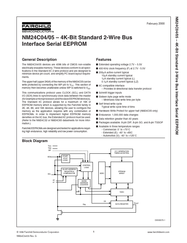
Block Diagram
VCC VSS WP SDA
START STOP LOGIC
SLAVE ADDRESS REGISTER &
PARATOR
CONTROL LOGIC
Features
I Extended operating voltage 2.7V
- 5.5V I 400 KHz clock frequency (F) at 2.7V
- 5.5V I 200µA active current typical
10µA standby current typical 1µA standby current typical (L) 0.1µA standby current typical (LZ) I IIC patible interface
- Provides bi-directional data transfer protocol I Schmitt trigger inputs I Sixteen byte page write mode
- Minimizes total write time per byte I Self timed write cycle Typical write cycle time of 6ms I Hardware Write Protect for upper half (NM24C05 only) I Endurance: 1,000,000 data changes I Data retention greater than 40 years I Packages available: 8-pin DIP, 8-pin SO, and 8-pin TSSOP I Available in three temperature ranges
- mercial: 0° to +70°C
- Extended (E):...