2N5951 Overview
Key Specifications
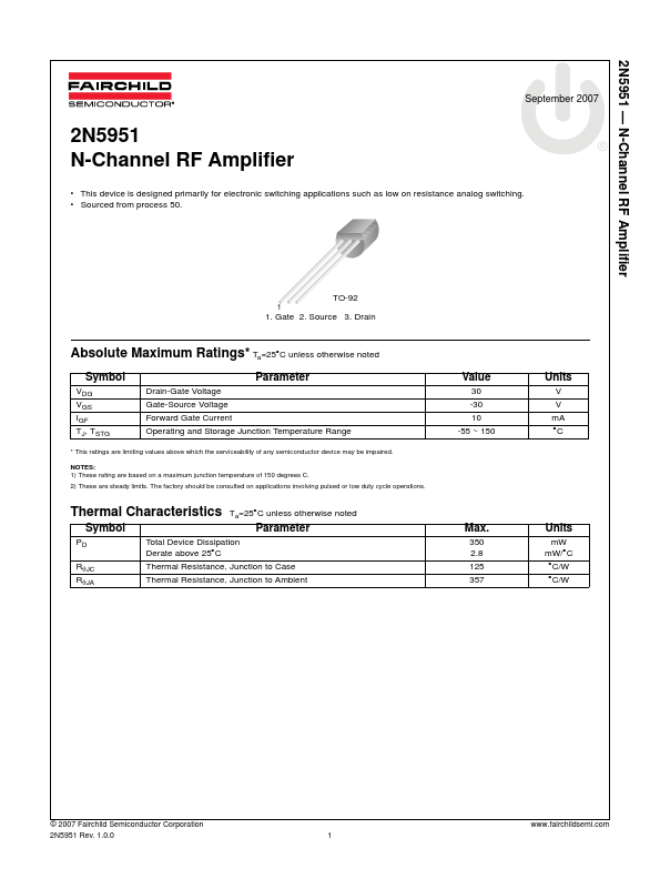
Pins: 3
Max Operating Temp: 150 °C
Min Operating Temp: -55 °C
Key Features
- This device is designed primarily for electronic switching applications such as low on resistance analog switching
- Sourced from process 50