74LVTH322374
74LVTH322374 is Low Voltage 32-Bit D-Type Flip-Flop manufactured by Fairchild Semiconductor.
Description
The LVTH322374 contains thirty-two non-inverting D-type flip-flops with 3-STATE outputs and is intended for bus oriented applications. The device is byte controlled. A buffered clock (CP) and Output Enable (OE) are mon to each byte and can be shorted together for full 32-bit operation. The LVTH322374 is designed with equivalent 25Ω series resistance in both the HIGH and LOW states of the output. This design reduces line noise in applications such as memory address drivers, clock drivers, and bus transceivers/transmitters. The LVTH322374 data inputs include bushold, eliminating the need for external pull-up resistors to hold unused inputs. These flip-flops are designed for low voltage (3.3V) VCC applications, but with the capability to provide a TTL interface to a 5V environment. The LVTH322374 is fabricated with an advanced Bi CMOS technology to achieve high speed operation similar to 5V ABT while maintaining a low power dissipation.
Features s Input and output interface capability to systems at 5V VCC s Bushold data inputs eliminate the need for external pullup resistors to hold unused inputs s Live insertion/extraction permitted s Power Up/Power Down high impedance provides glitchfree bus loading s Outputs include equivalent series resistance of 25Ω to make external termination resistors unnecessary and reduce overshoot and undershoot s ESD performance: Human-body model > 2000V Machine model > 200V Charged-device model > 1000V s Packaged in plastic Fine-Pitch Ball Grid Array (FBGA) (Preliminary)
Ordering Code:
Order Number 74LVTH322374GX (Note 1) Package Number BGA96A (Preliminary) Package Description
96-Ball Fine-Pitch Ball Grid Array (FBGA), JEDEC MO-205, 5.5mm Wide [Tape and Reel]
Note 1: BGA package available in Tape and Reel only.
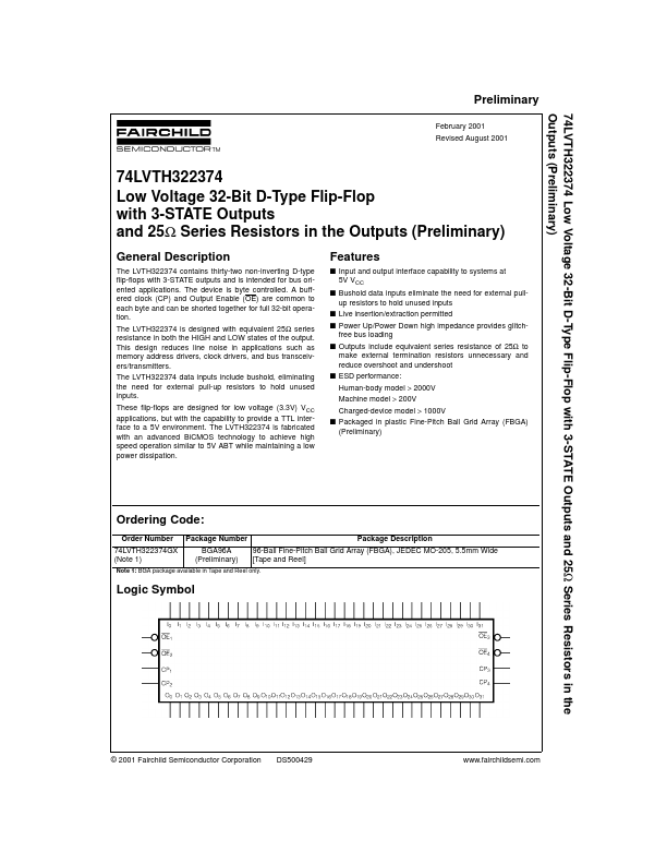
Logic Symbol
© 2001 Fairchild Semiconductor Corporation
DS500429
.fairchildsemi.
Preliminary 74LVTH322374 Connection Diagram Pin Descriptions for FBGA
Pin Names OEn CPn I0- I31 O0- O31 Description
Output Enable...