FDMC610P
Overview
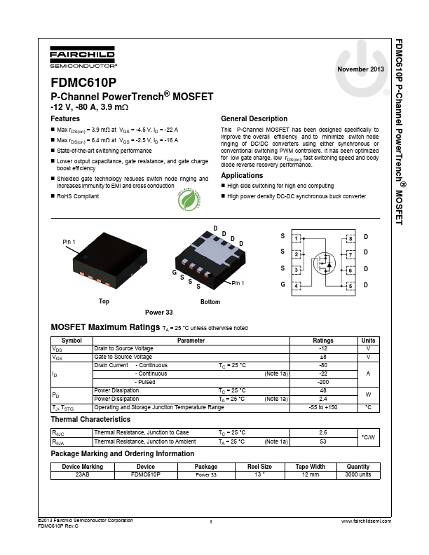
This P-Channel MOSFET has been designed specifically to improve the overall efficiency and to minimize switch node ringing of DC/DC converters using either synchronous or conventional switching PWM controllers. It has been optimized for low gate charge, low rDS(on), fast switching speed and body diode reverse recovery performance.
- Max rDS(on) = 3.9 mΩ at VGS = -4.5 V, ID = -22 A
- Max rDS(on) = 6.4 mΩ at VGS = -2.5 V, ID = -16 A
- State-of-the-art switching performance
- Lower output capacitance, gate resistance, and gate charge boost efficiency
- Shielded gate technology reduces switch node ringing and increases immunity to EMI and cross conduction
- RoHS Compliant November 2013