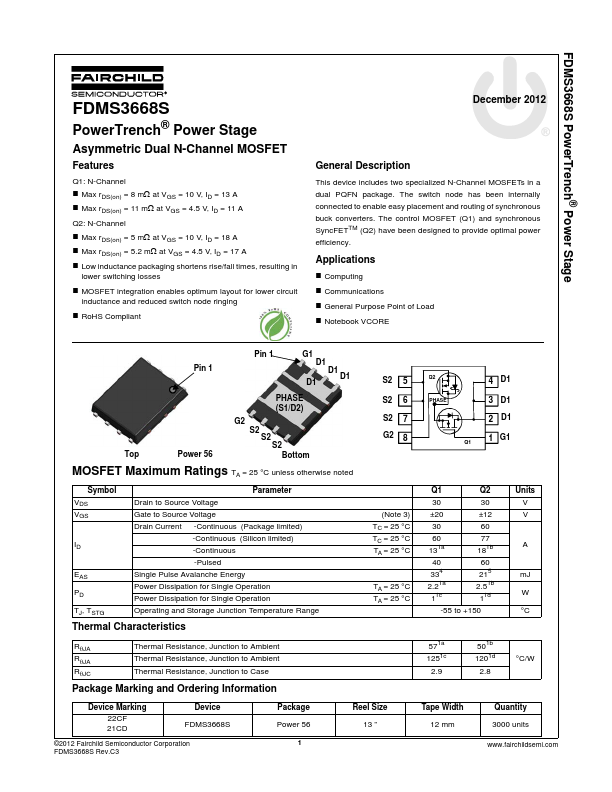
FDMS3668S
Features
Q1: N-Channel
- Max r DS(on) = 8 mΩ at VGS = 10 V, ID = 13 A
- Max r DS(on) = 11 mΩ at VGS = 4.5 V, ID = 11 A
Q2: N-Channel
- Max r DS(on) = 5 mΩ at VGS = 10 V, ID = 18 A
- Max r DS(on) = 5.2 mΩ at VGS = 4.5 V, ID = 17 A
- Low inductance packaging shortens rise/fall times, resulting in lower switching losses
- MOSFET integration enables optimum layout for lower circuit inductance and reduced switch node ringing
- Ro HS pliant
December 2012
General Description
This device includes two specialized N-Channel MOSFETs in a dual PQFN package. The switch node has been internally connected to enable easy placement and routing of synchronous buck converters. The control MOSFET (Q1) and synchronous Sync FETTM (Q2) have been designed to provide optimal power efficiency.
Applications
- puting
- munications
- General Purpose Point of Load
- Notebook VCORE
Pin...