FDMS9620S
FDMS9620S is 30V Dual N-Channel PowerTrench MOSFET manufactured by Fairchild Semiconductor.
Features
Q1: N-Channel
- Max r DS(on) = 21.5m: at VGS = 10V, ID = 7.5A
- Max r DS(on) = 29.5m: at VGS = 4.5V, ID = 6.5A Q2: N-Channel
- Max r DS(on) = 13m: at VGS = 10V, ID = 10A
- Max r DS(on) = 17m: at VGS = 4.5V, ID = 8.5A
- Low Qg high side MOSFET
- Low r DS(on) low side MOSFET
- Thermally efficient dual Power 56 package
- Pinout optimized for simple PCB design
- Ro HS pliant
General Description
This device includes two specialized MOSFETs in a unique dual Power 56 package. It is designed to provide an optimal Synchronous Buck power stage in terms of efficiency and PCB utilization. The low switching loss "High Side" MOSFET is plemented by a Low Conduction Loss "Low Side" Sync FET.
Applications
Synchronous Buck Converter for:
- Notebook System Power
- General Purpose Point of Load
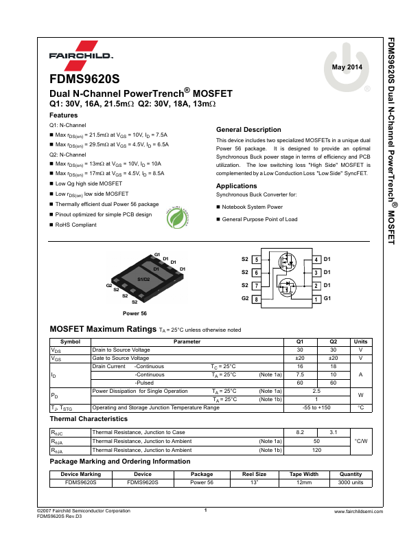
G1 D1 D1
D1 D1
S1/D2 G2
S2 S2 S2
Power 56
S2...