FDP6035AL
FDP6035AL is N-Channel MOSFET manufactured by Fairchild Semiconductor.
Description
This N-Channel Logic Level MOSFET has been designed specifically to improve the overall efficiency of DC/DC converters using either synchronous or conventional switching PWM controllers. These MOSFETs feature faster switching and lower gate charge than other MOSFETs with parable RDS(on) specifications. The result is a MOSFET that is easy and safer to drive (even at very high frequencies), and DC/DC power supply designs with higher overall efficiency.
Features
48A, 30 V. RDS(ON) = 0.0125 Ω @ VGS = 10 V, RDS(ON) = 0.017 Ω @ VGS = 4.5 V. Critical DC electrical parameters specified at elevated temperature. Rugged internal source-drain diode can eliminate the need for an external Zener diode transient suppressor. High performance trench technology for extremely low RDS(ON). 175°C maximum junction temperature rating.
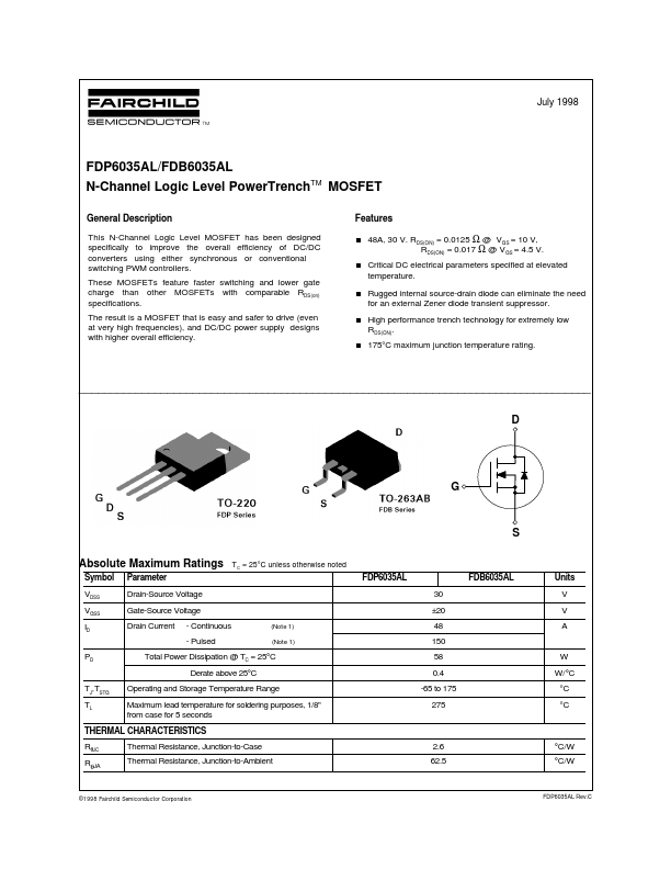
S Absolute Maximum Ratings
Symbol VDSS VGSS ID PD Parameter Drain-Source Voltage Gate-Source Voltage Drain Current
- Continuous
- Pulsed
(Note 1) (Note 1)
T C = 25°C unless otherwise noted
FDP6035AL 30 ±20 48 150 58 0.4 -65 to 175 275
FDB6035AL
Units V V A
Total Power Dissipation @ TC = 25°C Derate above 25°C
W W/°C °C °C
TJ,TSTG TL
Operating and Storage Temperature Range Maximum lead temperature for soldering purposes, 1/8" from case for 5 seconds
THERMAL CHARACTERISTICS RθJC RθJA Thermal Resistance, Junction-to-Case Thermal Resistance, Junction-to-Ambient 2.6 62.5 °C/W °C/W
© 1998 Fairchild Semiconductor Corporation
FDP6035AL Rev.C
Electrical Characteristics (TC = 25°C unless otherwise noted)
Symbol Parameter Conditions Min Typ Max Unit DRAIN-SOURCE AVALANCHE RATINGS (Note 1) W DSS IAR Single Pulse Drain-Source Avalanche Energy Maximum Drain-Source Avalanche Current VDD = 15 V, ID = 48 A 130 48 m J A
OFF CHARACTERISTICS BVDSS Drain-Source Breakdown Voltage VGS = 0 V, ID = 250 µA ID = 250 µA, Referenced to 25 C VDS = 24 V, VGS = 0 V VGS = 20 V,...