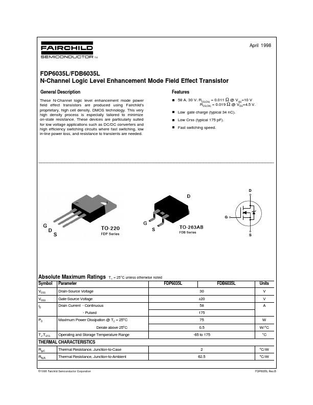
FDP6035L
FDP6035L is N-Channel MOSFET manufactured by Fairchild Semiconductor.
Description
These N-Channel logic level enhancement mode power field effect transistors are produced using Fairchild's proprietary, high cell density, DMOS technology. This very high density process is especially tailored to minimize on-state resistance. These devices are particularly suited for low voltage applications such as DC/DC converters and high efficiency switching circuits where fast switching, low in-line power loss, and resistance to transients are needed.
Features
58 A, 30 V. RDS(ON) = 0.011 Ω @ VGS=10 V RDS(ON) = 0.019 Ω @ VGS=4.5 V. Low gate charge (typical 34 n C). Low Crss (typical 175 p F). Fast switching speed.
Absolute Maximum Ratings
Symbol VDSS VGSS ID PD Parameter Drain-Source Voltage Gate-Source Voltage Drain Current
- Continuous
- Pulsed
T C = 25°C unless otherwise noted
FDP6035L 30 ±20 58 175 75 0.5 -65 to 175
FDB6035L
Units V V A
Maximum Power Dissipation @ TC = 25°C Derate above 25°C
W W/°C °C
TJ,TSTG RθJC RθJA
Operating and Storage Temperature Range
THERMAL CHARACTERISTICS Thermal Resistance, Junction-to-Case Thermal Resistance, Junction-to-Ambient 2 62.5 °C/W °C/W
© 1998 Fairchild Semiconductor Corporation
FDP6035L Rev.B
Electrical Characteristics
Symbol Parameter
T C = 25°C unless otherwise noted)
Conditions
Min
Typ
Max
Unit
DRAIN-SOURCE AVALANCHE RATINGS (Note 1)
W DSS IAR BVDSS Single Pulse Drain-Source Avalanche Energy Maximum Drain-Source Avalanche Current VDD = 15 V, ID = 21 A 150 21 m J A
OFF CHARACTERISTICS Drain-Source Breakdown Voltage VGS = 0 V, ID = 250 µA ID = 250 µA, Referenced to 25 o C VDS = 24 V, VGS = 0 V VGS = 20 V, VDS = 0 V VGS = -20 V, VDS = 0 V VDS = VGS, ID = 250 µA ID = 250 µA, Referenced to 25 C VGS = 10 V, ID = 26 A TJ =125 °C VGS = 4.5 V, ID = 21 A ID(on) ID(on) g FS On-State Drain Current On-State Drain Current Forward Transconductance VGS = 10 V, VDS = 10 V VGS = 4.5 V, VDS = 10 V VDS = 10 V, ID = 26...