FDS8672S Overview
Key Specifications
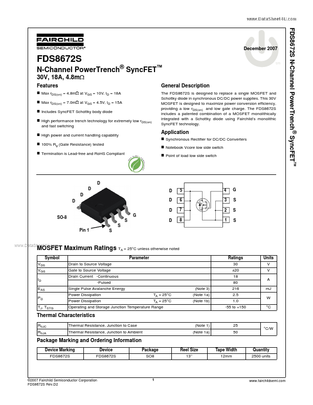
Package: SOIC
Mount Type: Surface Mount
Pins: 8
Height: 1.5 mm
Description
tm The FDS8672S is designed to replace a single MOSFET and Schottky diode in synchronous DC/DC power supplies. This 30V MOSFET is designed to maximize power conversion efficiency, providing a low rDS(on) and low gate charge.
Key Features
- Max rDS(on) = 4.8mΩ at VGS = 10V, ID = 18A
- Max rDS(on) = 7.0mΩ at VGS = 4.5V, ID = 15A
- Includes SyncFET Schottky body diode
- High performance trench technology for extremely low rDS(on) and fast switching
- High power and current handling capability