• Part: FIN1022
  • Description: 2 X 2 LVDS High Speed Crosspoint Switch
  • Manufacturer: Fairchild Semiconductor
  • Size: 547.04 KB
Download FIN1022 Datasheet PDF
Fairchild Semiconductor
FIN1022
FIN1022 is 2 X 2 LVDS High Speed Crosspoint Switch manufactured by Fairchild Semiconductor.
- Part of the FIN comparator family.
FIN1022 2 X 2 LVDS High Speed Crosspoint Switch September 2001 Revised December 2001 FIN1022 2 X 2 LVDS High Speed Crosspoint Switch General Description 
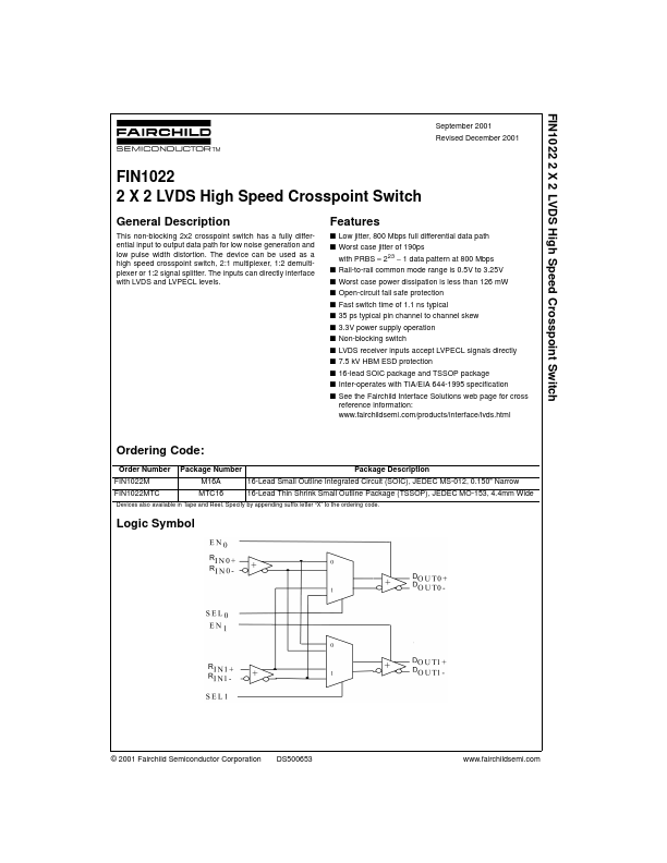
This non-blocking 2x2 crosspoint switch has a fully differential input to output data path for low noise generation and low pulse width distortion. The device can be used as a high speed crosspoint switch, 2:1 multiplexer, 1:2 demultiplexer or 1:2 signal splitter. The inputs can directly interface with LVDS and LVPECL levels. Features s Low jitter, 800 Mbps full differential data path s Worst case jitter of 190ps with PRBS = 223 - 1 data pattern at 800 Mbps s Rail-to-rail mon mode range is 0.5V to 3.25V s Worst case power dissipation is less than 126 m W s Open-circuit fail safe protection s Fast switch time of 1.1 ns typical s 35 ps typical pin channel to channel skew s 3.3V power supply operation s Non-blocking switch s LVDS receiver inputs accept LVPECL signals directly s 7.5 k V HBM ESD protection s 16-lead SOIC package and TSSOP package s Inter-operates with TIA/EIA 644-1995 specification s See the Fairchild Interface Solutions web page for cross reference information: .fairchildsemi./products/interface/lvds.html Ordering Code: Order Number FIN1022M FIN1022MTC Package Number M16A MTC16 Package Description 16-Lead Small Outline Integrated Circuit (SOIC), JEDEC MS-012, 0.150" Narrow 16-Lead Thin Shrink Small Outline Package (TSSOP), JEDEC MO-153, 4.4mm Wide Devices also available in Tape and Reel. Specify by appending suffix letter “X” to the ordering code. Logic Symbol © 2001 Fairchild Semiconductor Corporation DS500653 .fairchildsemi. Connection Diagram Pin Descriptions Pin Name RIN0+, RIN1+ RIN0- , RIN1- Description LVDS non-inverting data inputs LVDS inverting data inputs DOUT0+, DOUT1+ LVDS non-inverting data outputs DOUT0- , DOUT1- LVDS inverting data outputs EN0 EN1 SEL0 SEL1 VCC GND LVTTL input for enabling DOUT0+/DOUT0- LVTTL input for enabling DOUT1+/DOUT1- LVTTL input...