FIN1049
FIN1049 is LVDS Dual Line Driver manufactured by Fairchild Semiconductor.
FIN1049 LVDS Dual Line Driver with Dual Line Receiver
March 2003 Revised March 2003
FIN1049 LVDS Dual Line Driver with Dual Line Receiver
General Description
This dual Driver-Receiver is designed for high speed interconnects utilizing Low Voltage Differential Signaling (LVDS) technology. The Driver accepts LVTTL inputs and translates them to LVDS outputs. The Receiver accepts LVDS inputs and translates them to LVTTL outputs. The LVDS levels have a typical differential output swing of 350m V which provide for low EMI at ultra low power dissipation even at high frequencies. The FIN1049 can accept LVPECL inputs for translating from LVPECL to LVDS. The En and Enb inputs are ANDed together to enable/disable the outputs. The enables are mon to all four outputs. A single line driver and single line receiver function is also available in the FIN1019.
Features s Greater than 400 Mbps data rate s 3.3V power supply operation s Low power dissipation s Fail safe protection for open-circuit conditions s Meets or exceeds the TIA/EIA-644-A LVDS standard s 16-pin TSSOP package saves space s Flow-through pinout simplifies PCB layout s Enable/Disable for all outputs s Industrial operating temperature range:
- 40°C to +85°C
Ordering Code:
Order Number Package Number
Package Description
FIN1049MTC
MTC16
16-Lead Thin Shrink Small Outline Package (TSSOP), JEDEC MO-153, 4.4mm Wide
Device also available in Tape and Reel. Specify by appending suffix letter “X” to the ordering code.
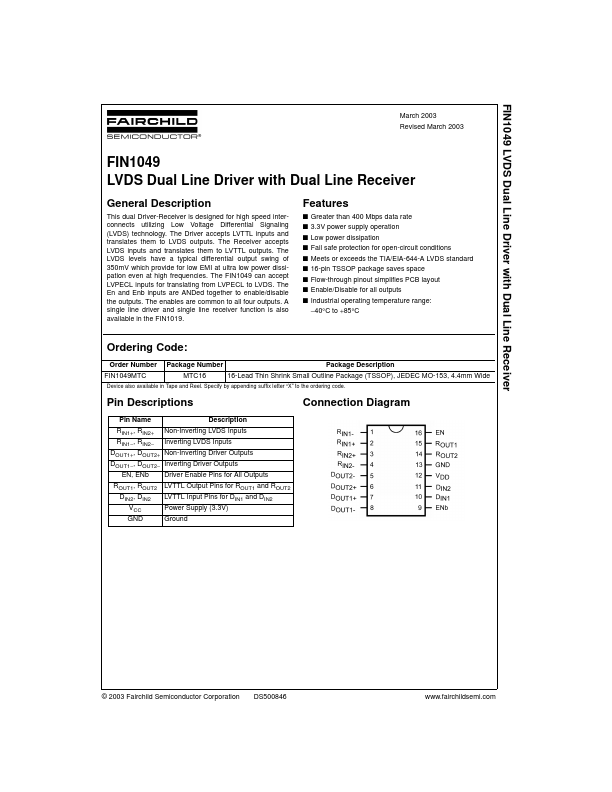
Pin Descriptions
Connection Diagram
Pin Name
Description
RIN1+, RIN2+ Non-Inverting LVDS Inputs RIN1- , RIN2- Inverting LVDS Inputs DOUT1+, DOUT2+ Non-Inverting Driver Outputs DOUT1- , DOUT2- Inverting Driver Outputs
EN, ENb Driver Enable Pins for All Outputs
ROUT1, ROUT2 DIN2, DIN2 VCC GND
LVTTL Output Pins for ROUT1 and ROUT2 LVTTL Input Pins for DIN1 and DIN2 Power Supply (3.3V)
Ground
© 2003 Fairchild Semiconductor Corporation DS500846
.fairchildsemi.
Function Table
Inputs...