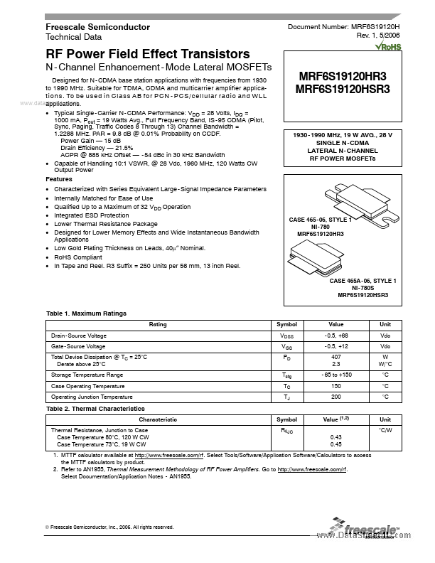
MRF6S19120HR3
MRF6S19120HR3 is RF Power Transistors manufactured by Freescale Semiconductor.
Freescale Semiconductor Technical Data
Document Number: MRF6S19120H Rev. 1, 5/2006
RF Power Field Effect Transistors
- Channel Enhancement
- Mode Lateral MOSFETs
Designed for N
- CDMA base station applications with frequencies from 1930 to 1990 MHz. Suitable for TDMA, CDMA and multicarrier amplifier applicat i o n s . To b e u s e d i n C l a s s A B f o r P C N
- P C S / c e l l u l a r r a d i o a n d W L L .. applications.
- Typical Single
- Carrier N
- CDMA Performance: VDD = 28 Volts, IDQ = 1000 m A, Pout = 19 Watts Avg., Full Frequency Band, IS
- 95 CDMA (Pilot, Sync, Paging, Traffic Codes 8 Through 13) Channel Bandwidth = 1.2288 MHz. PAR = 9.8 d B @ 0.01% Probability on CCDF. Power Gain
- 15 d B Drain Efficiency
- 21.5% ACPR @ 885 k Hz Offset
- - 54 d Bc in 30 k Hz Bandwidth
- Capable of Handling 10:1 VSWR, @ 28 Vdc, 1960 MHz, 120 Watts CW Output Power Features
- Characterized with Series Equivalent Large
- Signal Impedance Parameters
- Internally Matched for Ease of Use
- Qualified Up to a Maximum of 32 VDD Operation
- Integrated ESD Protection
- Lower Thermal Resistance Package
- Designed for Lower Memory Effects and Wide Instantaneous Bandwidth Applications
- Low Gold Plating Thickness on Leads, 40μ″ Nominal.
- Ro HS pliant
- In Tape and Reel. R3 Suffix = 250 Units per 56 mm, 13 inch Reel.
MRF6S19120HR3 MRF6S19120HSR3
- 1990 MHz, 19 W AVG., 28 V SINGLE N
- CDMA LATERAL N
- CHANNEL RF POWER...