MRF6S21050LSR3
MRF6S21050LSR3 is RF Power Field Effect Transistors manufactured by Freescale Semiconductor.
- Part of the MRF6S21050LR3 comparator family.
- Part of the MRF6S21050LR3 comparator family.
..
Freescale Semiconductor Technical Data
MRF6S21050L Rev. 0, 3/2005
RF Power Field Effect Transistors
- Channel Enhancement
- Mode Lateral MOSFETs
Designed for W
- CDMA base station applications with frequencies from 2110 to 2170 MHz. Suitable for TDMA, CDMA and multicarrier amplifier applicat i o n s . To b e u s e d i n C l a s s A B f o r P C N
- P C S / c e l l u l a r r a d i o a n d W L L applications.
- Typical 2
- carrier W
- CDMA Performance: VDD = 28 Volts, IDQ = 450 m A, Pout = 11.5 Watts Avg., Full Frequency Band, Channel Bandwidth = 3.84 MHz, PAR = 8.5 d B @ 0.01% Probability on CCDF. Power Gain
- 16 d B Drain Efficiency
- 27.7% IM3 @ 10 MHz Offset
- - 37 d Bc @ 3.84 MHz Channel Bandwidth ACPR @ 5 MHz Offset
- - 40 d Bc @ 3.84 MHz Channel Bandwidth
- Capable of Handling 10:1 VSWR, @ 28 Vdc, 2140 MHz, 50 Watts CW Output Power
- Characterized with Series Equivalent Large
- Signal Impedance Parameters
- Internally Matched, Controlled Q, for Ease of Use
- Qualified Up to a Maximum of 32 VDD Operation
- Integrated ESD Protection
- Designed for Lower Memory Effects and Wide Instantaneous Bandwidth Applications
- Low Gold Plating Thickness on Leads, 40µ″ Nominal.
- In Tape and Reel. R3 Suffix = 250 Units per 32 mm, 13 inch Reel.
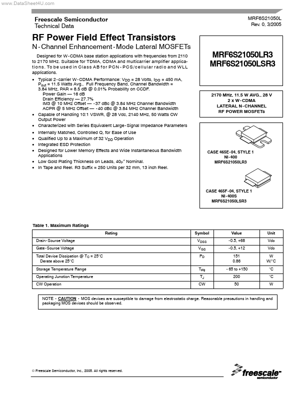
MRF6S21050LR3 MRF6S21050LSR3
2170 MHz, 11.5 W AVG., 28 V 2 x W
- CDMA LATERAL N
- CHANNEL RF POWER MOSFETs
CASE 465E
- 04, STYLE 1 NI
- 400 MRF6S21050LR3
CASE 465F
- 04, STYLE 1 NI
- 400S MRF6S21050LSR3
Table 1. Maximum Ratings
Rating Drain- Source Voltage Gate- Source Voltage Total Device Dissipation @ TC = 25°C Derate above 25°C Storage Temperature Range Operating Junction Temperature CW Operation Symbol VDSS VGS PD Tstg TJ CW Value
- 0.5, +68
- 0.5, +12 151...