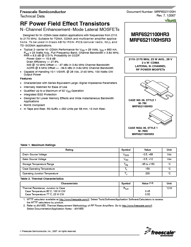
MRF6S21100HSR3
MRF6S21100HSR3 is RF Power Field Effect Transistors manufactured by Freescale Semiconductor.
- Part of the MRF6S21100HR3 comparator family.
- Part of the MRF6S21100HR3 comparator family.
Features
- Characterized with Series Equivalent Large
- Signal Impedance Parameters
- Internally Matched for Ease of Use
- Qualified Up to a Maximum of 32 VDD Operation
- Integrated ESD Protection
- Designed for Lower Memory Effects and Wide Instantaneous Bandwidth Applications
- Ro HS pliant
- In Tape and Reel. R3 Suffix = 250 Units per 56 mm, 13 inch Reel.
MRF6S21100HR3 MRF6S21100HSR3
- 2170 MHz, 23 W AVG., 28 V 2 x W
- CDMA LATERAL N
- CHANNEL RF POWER MOSFETs
CASE 465
- 06, STYLE 1 NI
- 780 MRF6S21100HR3
CASE 465A
- 06, STYLE 1 NI
- 780S MRF6S21100HSR3
Table 1. Maximum Ratings
Rating Drain
- Source Voltage Gate
- Source Voltage Storage Temperature Range Case Operating Temperature Operating Junction Temperature Symbol VDSS VGS Tstg Tc TJ Value
- 0.5, +68
- 0.5, +12
- 65 to +150 150 200 Unit Vdc Vdc °C °C °C
Table 2. Thermal Characteristics
Characteristic Thermal Resistance, Junction to Case Case Temperature 80°C, 100 W CW Case Temperature 77°C, 23 W CW Symbol RθJC Value (1,2) 0.45 0.52 Unit °C/W
1. MTTF calculator available at http://.freescale./rf. Select Tools/Software/Application Software/Calculators to access the MTTF calculators by product. 2. Refer to AN1955, Thermal Measurement Methodology of RF Power Amplifiers. Go to http://.freescale./rf. Select Documentation/Application Notes
- AN1955.
© Freescale Semiconductor, Inc., 2007. All rights reserved.
MRF6S21100HR3 MRF6S21100HSR3 1
RF Device Data Freescale Semiconductor
Table 3. ESD Protection Characteristics
Test Methodology Human Body Model (per JESD22
- A114) Machine Model (per EIA/JESD22
- A115) Charge Device Model (per JESD22
- C101) Class 3A (Minimum) A (Minimum) IV (Minimum)
Table 4. Electrical Characteristics (TC = 25°C unless otherwise...