MBM29DS163TE
MBM29DS163TE is (MBM29DS163BE/TE) FLASH MEMORY CMOS 16 M (2 M X 8/1 M X 16) BIT manufactured by Fujitsu Semiconductor Limited.
..
FUJITSU SEMICONDUCTOR DATA SHEET
DS05-20891-4E
FLASH MEMORY
CMOS
16 M (2 M × 8/1 M × 16) BIT Dual Operation
MBM29DS163TE/BE10 s DESCRIPTION
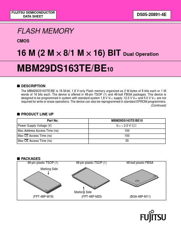
The MBM29DS163TE/BE is 16 M-bit, 1.8 V-only Flash memory organized as 2 M bytes of 8 bits each or 1 M words of 16 bits each. The device is offered in 48-pin TSOP (1) and 48-ball FBGA packages. This device is designed to be programmed in system with standard system 1.8 V VCC supply. 12.0 V VPP and 5.0 V VCC are not required for write or erase operations. The device can also be reprogrammed in standard EPROM programmers. (Continued) s PRODUCT LINE UP
Part No. Power Supply Voltage (V) Max Address Access Time (ns) Max CE Access...