GE02N60
GE02N60 is N-CHANNEL ENHANCEMENT MODE POWER MOSFET manufactured by GTM.
Description
The GE02N60 provide the designer with the best bination of fast switching. The TO-220 package is universally preferred for all mercial-industrial applications. The device is suited for DC-DC, DC-AC converters for tele, industrial and consumer environment.
- Dynamic dv/dt Rating
- Simple Drive Requirement
- Repetitive Avalanche Rated
- Fast Switching
Features
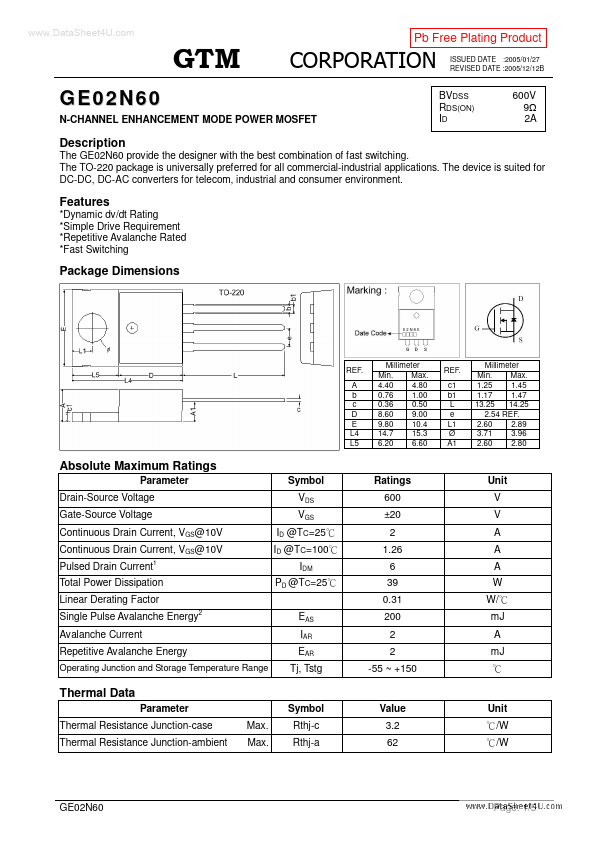
Package Dimensions
REF. A b c D E L4 L5
Millimeter Min. Max. 4.40 4.80 0.76 1.00 0.36 0.50 8.60 9.00 9.80 10.4 14.7 15.3 6.20 6.60
REF. c1 b1 L e L1 Ø A1
Millimeter Min. Max. 1.25 1.45 1.17 1.47 13.25 14.25 2.54 REF. 2.60 2.89 3.71 3.96 2.60 2.80
Absolute Maximum Ratings
Parameter Drain-Source Voltage Gate-Source Voltage Continuous Drain Current, VGS@10V Continuous Drain Current, VGS@10V Pulsed Drain Current
Symbol VDS VGS ID @TC=25 ID @TC=100 IDM PD @TC=25
Ratings 600 ±20 2 1.26 6 39 0.31 200 2 2 -55 ~ +150
Unit V V A A A W W/ m J A m J
Total Power Dissipation Linear Derating Factor Single Pulse Avalanche Energy Avalanche Current Repetitive Avalanche Energy
Operating Junction and Storage Temperature Range
EAS IAR EAR Tj, Tstg
Thermal Data
Parameter Thermal Resistance Junction-case Thermal Resistance Junction-ambient Max. Max. Symbol Rthj-c Rthj-a Value 3.2 62 Unit /W /W
Page: 1/5
..
ISSUED DATE :2005/01/27 REVISED DATE :2005/12/12B
Electrical Characteristics (Tj = 25
Parameter Drain-Source Breakdown Voltage
Breakdown Voltage Temperature Coefficient unless otherwise specified)
Min. 600 2.0 Typ. 0.6 0.8 13.9 1.9 8.2 8.8 10 21.3 8.8 155 27 14 Max. 4.0 ±100 100 500 9.0 p F ns n C Unit V V/ V S n A u A u A Test Conditions VGS=0, ID=250u A Reference to 25 , ID=1m A VDS=VGS, ID=250u A VDS=10V, ID=1A VGS= ±20V VDS=600V, VGS=0 VDS=480V, VGS=0 VGS=10V, ID=1A ID=2A VDS=480V VGS=10V VDD=300V ID=2A VGS=10V RG=10 RD=150 VGS=0V VDS=25V f=1.0MHz
Symbol BVDSS
BVDSS / Tj
Gate Threshold Voltage Forward Transconductance Gate-Source Leakage Current
Drain-Source Leakage Current(Tj=25 ) Drain-Source...