Datasheet4U Logo Datasheet4U.com

GT2531 - N AND P-CHANNEL ENHANCEMENT MODE POWER MOSFET

General Description

The GT2531 utilized advanced processing techniques to achieve the lowest possible on-resistance, extremely efficient and cost-effectiveness device.

Key Features

  • Low Gate Change.
  • Low On-resistance.
  • RoHS Compliant Package Dimensions REF. A B C D E F Millimeter Min. 2.70 2.60 1.40 0.30 0 0° Max. 3.10 3.00 1.80 0.55 0.10 10° REF. G H I J K L Dimensions Millimeter 1.90 REF. 1.20 REF. 0.12 REF. 0.37 REF. 0.60 REF. 0.95 REF. Absolute Maximum Ratings Parameter Drain-Source Voltage Gate-Source Voltage Continuous Drain Current Continuous Drain Current Pulsed Drain Current 1 3 3 Symbol VDS VGS ID @TA=25 ID @TA=70 IDM PD @TA=25 Tj, Tstg Rating.

📥 Download Datasheet

Datasheet Details

Part number GT2531
Manufacturer GTM
File Size 415.61 KB
Description N AND P-CHANNEL ENHANCEMENT MODE POWER MOSFET
Datasheet download datasheet GT2531 Datasheet

Full PDF Text Transcription (Reference)

The following content is an automatically extracted verbatim text from the original manufacturer datasheet and is provided for reference purposes only.

View original datasheet text
www.DataSheet4U.com Pb Free Plating Product ISSUED DATE :2006/01/23 REVISED DATE : GT2531 N AND P-CHANNEL ENHANCEMENT MODE POWER MOSFET Description 
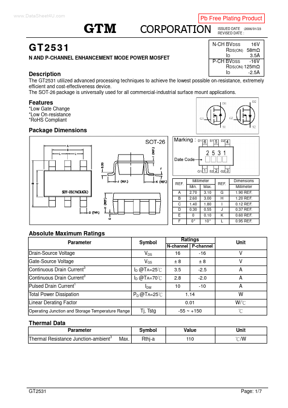
N-CH BVDSS 16V N-CH RDS(ON) 58m N-CH ID 3.5A P-CH BVDSS -16V N-CH RDS(ON) 125m N-CH ID -2.5A The GT2531 utilized advanced processing techniques to achieve the lowest possible on-resistance, extremely efficient and cost-effectiveness device. The SOT-26 package is universally used for all commercial-industrial surface mount applications. Features *Low Gate Change *Low On-resistance *RoHS Compliant Package Dimensions REF. A B C D E F Millimeter Min. 2.70 2.60 1.40 0.30 0 0° Max. 3.10 3.00 1.80 0.55 0.10 10° REF. G H I J K L Dimensions Millimeter 1.90 REF. 1.20 REF. 0.12 REF. 0.37 REF. 0.60 REF. 0.95 REF.