BS108
BS108 is DMOS Transistors manufactured by General Semiconductor.
FEATURES
- -
- -
- -
- -
- -
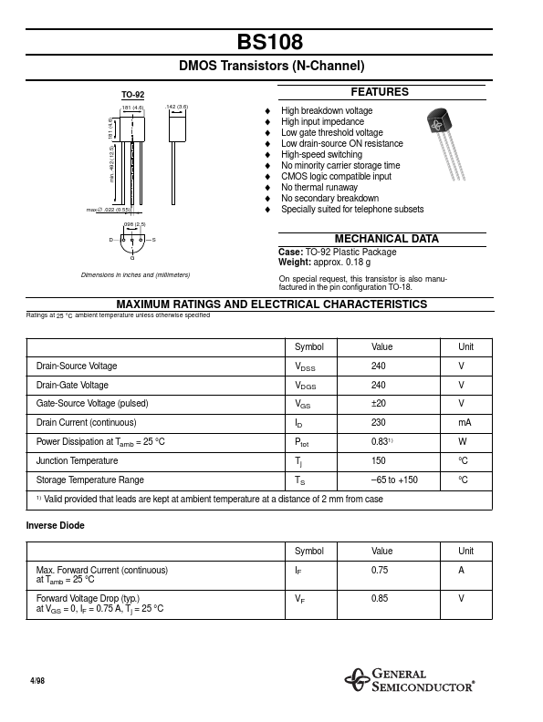
High breakdown voltage High input impedance Low gate threshold voltage Low drain-source ON resistance High-speed switching No minority carrier storage time CMOS logic patible input No thermal runaway No secondary breakdown Specially suited for telephone subsets max. ∅ .022 (0.55) .098 (2.5) D G S
MECHANICAL DATA
Case: TO-92 Plastic Package Weight: approx. 0.18 g
On special request, this transistor is also manufactured in the pin configuration TO-18.
Dimensions in inches and (millimeters)
MAXIMUM RATINGS AND ELECTRICAL CHARACTERISTICS
Ratings at 25 °C ambient temperature unless otherwise specified
Symbol Drain-Source Voltage Drain-Gate Voltage Gate-Source Voltage (pulsed) Drain Current (continuous) Power Dissipation at Tamb = 25 °C Junction Temperature Storage Temperature Range
1)
Value 240 240 ±20 230 0.831) 150
- 65 to +150
Unit V V V m A W °C °C
VDSS VDGS VGS ID Ptot Tj TS
Valid provided that leads are kept at ambient temperature at a distance of 2 mm from case
Inverse Diode Symbol Max. Forward Current (continuous) at Tamb = 25 °C Forward Voltage Drop (typ.) at VGS = 0, IF = 0.75 A, Tj = 25 °C IF VF Value 0.75 0.85 Unit A V
4/98
ELECTRICAL CHARACTERISTICS
Ratings at 25 °C ambient temperature unless otherwise specified
Symbol Drain-Source Breakdown Voltage at ID = 100 µA, VGS = 0 Gate-Body Leakage Current at VGS = 15 V, VDS = 0 Drain Cutoff Current at VDS = 130 V, VGS = 0 at VDS = 70 V, VGS = 0.2 V Gate-Source Threshold Voltage at VGS = VDS, ID = 1 m A Drain-Source ON Resistance at VGS = 2.8 V, ID = 100 m A Thermal Resistance Junction to Ambient Air Capacitance at VDS = 20 V, VGS = 0, f = 1 MHz Input Capacitance Output Capacitance Feedback Capacitance Switching Times at VGS = 10 V, VDS = 10 V, RD = 100 Ω Turn-On Time Turn-Off Time
1)
Min. 240
- Typ. 250
- Max.
- 10
Unit V n A
V(BR)DSS IGSS
IDSS IDSX VGS(th) RDS(ON) Rth JA
- - 0.8
- -
- - 1.5 5.5
- 1 25 2.5 8 1501)
µA µA V Ω K/W
Ci SS COSS Cr SS
- -...