BS108
BS108 is 200 VOLTS N-CHANNEL TMOS manufactured by Motorola Semiconductor.
MOTOROLA
SEMICONDUCTOR TECHNICAL DATA
Order this document by BS108/D
Logic Level TMOS
®
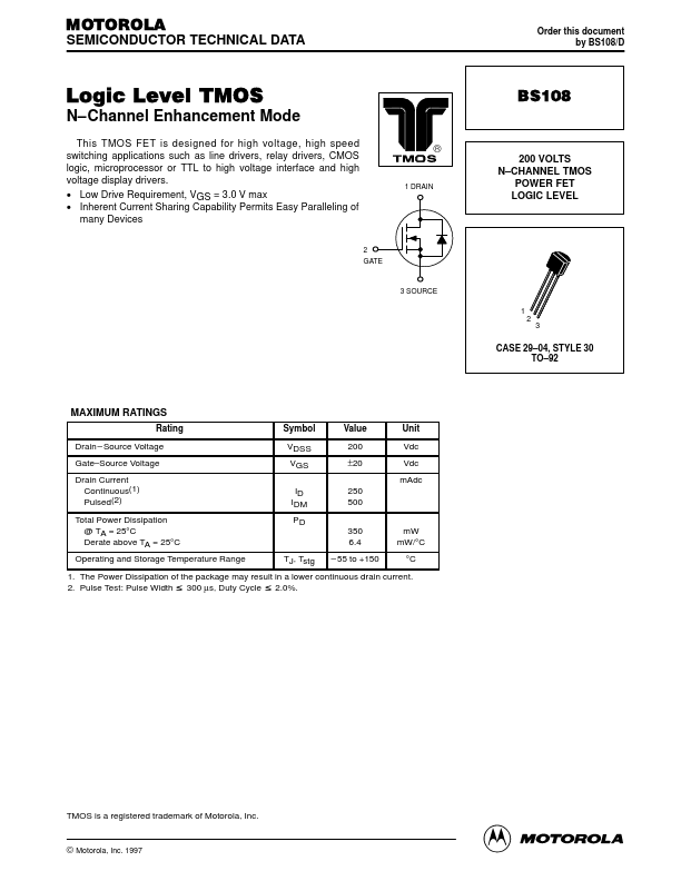
1 DRAIN
N- Channel Enhancement Mode
This TMOS FET is designed for high voltage, high speed switching applications such as line drivers, relay drivers, CMOS logic, microprocessor or TTL to high voltage interface and high voltage display drivers.
- Low Drive Requirement, VGS = 3.0 V max
- Inherent Current Sharing Capability Permits Easy Paralleling of many Devices
2 GATE 3 SOURCE
1 2 3
200 VOLTS N- CHANNEL TMOS POWER FET LOGIC LEVEL
CASE 29- 04, STYLE 30 TO- 92
MAXIMUM RATINGS
Rating Drain
- Source Voltage Gate- Source Voltage Drain Current Continuous(1) Pulsed(2) Total Power Dissipation @ TA = 25°C Derate above TA = 25°C Operating and Storage Temperature Range Symbol VDSS VGS ID IDM PD 350 6.4 TJ, Tstg
- 55 to +150 m W m W/°C °C Value 200 ±20 250 500 Unit Vdc Vdc m Adc
1. The Power Dissipation of the package may result in a lower continuous drain current. 2. Pulse Test: Pulse Width 300 µs, Duty Cycle 2.0%. v v
TMOS is a registered trademark of Motorola, Inc.
© Motorola, Inc. 1997
ELECTRICAL CHARACTERISTICS (TA = 25°C unless otherwise noted)
Characteristic Symbol Min Typ Max Unit
OFF CHARACTERISTICS
Drain- Source Breakdown Voltage (VGS = 0, ID = 10 µA) Zero Gate Voltage Drain Current (VDSS = 130 Vdc, VGS = 0) Gate- Body Leakage Current (VGS = 15 Vdc, VDS = 0) V(BR)DSS 200 IDSS
- IGSSF
- - 10
- 30 n Adc
- - n Adc Vdc
ON CHARACTERISTICS (2)
Gate Threshold Voltage (ID = 1.0 m A, VDS = VGS) Static Drain- to- Source On- Resistance (VGS = 2.0 Vdc, ID = 50 m A) (VGS = 2.8 Vdc, ID = 100 m A) Drain Cutoff Current (VGS = 0.2 V, VDS = 70 V) VGS(th) 0.5 r DS(on)
- - IDSX
- - 25
- - 10 8.0
- 1.5 Ohms Vdc m A
DYNAMIC CHARACTERISTICS
Input Capacitance (VDS = 25 V, VGS = 0, f = 1.0 MHz) Output Capacitance (VDS = 25 V, VGS = 0, f = 1.0 MHz) Reverse Transfer Capacitance (VDS = 25 V, VGS = 0, f = 1.0 MHz) Ciss
- Coss
- Crss
- -...