High Density Cell Design for Ultra Low On-Resistance.
Specially Designed for Low Voltage DC/DC Converters.
Fast Switching for High Efficiency
Maximum Ratings and Thermal Characteristics (T
Parameter Drain-Source Voltage Gate-Source Voltage Continuous Drain Current Pulsed Drain Current Maximum Power Dissipation TA = 25°C TA = 70°C
(1)
A
= 25°C unless otherwise noted)
Symbol VDS VGS ID IDM PD TJ, Tstg RθJA
Limit.
Full PDF Text Transcription for GF4435 (Reference)
Note: Below is a high-fidelity text extraction (approx. 800 characters) for
GF4435. For precise diagrams, and layout, please refer to the original PDF.
www.DataSheet4U.com GF4435 P-Channel Enhancement-Mode MOSFET H C N T E TRE NF E G
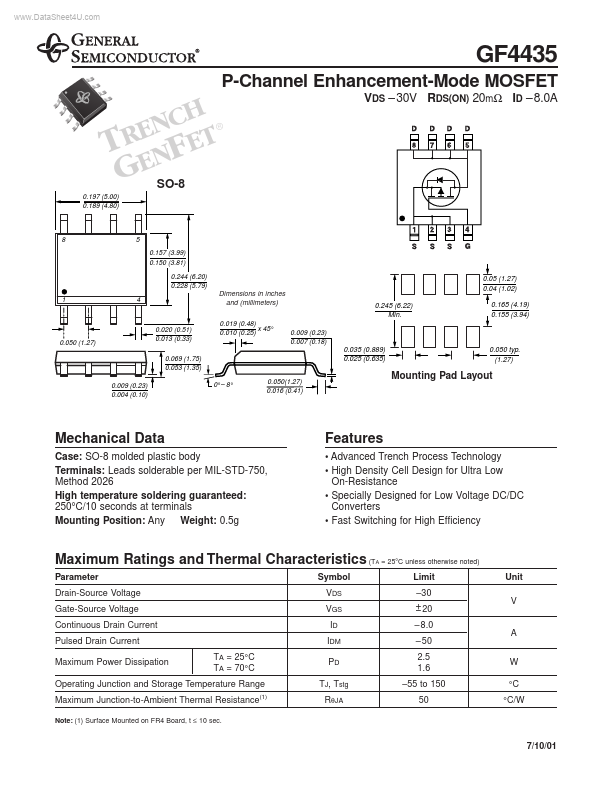
 SO-8 0.197 (5.00) 0.189 (4.80) 8 5 0.157 (3.99) 0.150 (3.81) 0.244 (6.20) 0.228 (5.79) 1...
View more extracted text
0.189 (4.80) 8 5 0.157 (3.99) 0.150 (3.81) 0.244 (6.20) 0.228 (5.79) 1 4 VDS –30V RDS(ON) 20mΩ ID –8.0A ® Dimensions in inches and (millimeters) 0.019 (0.48) x 45 ° 0.010 (0.25) 0.05 (1.27) 0.04 (1.02) 0.245 (6.22) Min. 0.009 (0.23) 0.007 (0.18) 0.165 (4.19) 0.155 (3.94) 0.050 (1.27) 0.020 (0.51) 0.013 (0.33) 0.069 (1.75) 0.053 (1.35) 0.009 (0.23) 0.004 (0.10) 0.035 (0.889) 0.025 (0.635) 0 °– 8 ° 0.050(1.27) 0.016 (0.41) 0.050 typ. (1.27) Mounting Pad Layout Mechanical Data Case: SO-8 molded plastic body Terminals: Leads solderable per MIL-STD-750, Method 2026 High temperature soldering guaranteed: 250°C/10 seconds at term
More Datasheets from General Semiconductor (now Vishay)