High Density Cell Design for Ultra Low On-Resistance.
Specially Designed for Low Voltage DC/DC Converters.
Fast Switching for High Efficiency
Maximum Ratings and Thermal Characteristics (T
Parameter Drain-Source Voltage Gate-Source Voltage Continuous Drain Current(1) Pulsed Drain Current Maximum Power Dissipation(1) TA = 25°C TA = 70°C
(1)
A
= 25°C unless otherwise noted)
Symbol VDS VGS ID IDM PD TJ, Tstg RθJA
Limit 60.
Full PDF Text Transcription for GF4450 (Reference)
Note: Below is a high-fidelity text extraction (approx. 800 characters) for
GF4450. For precise diagrams, and layout, please refer to the original PDF.
www.DataSheet4U.com GF4450 N-Channel Enhancement-Mode MOSFET H C N T E TRE NF E G
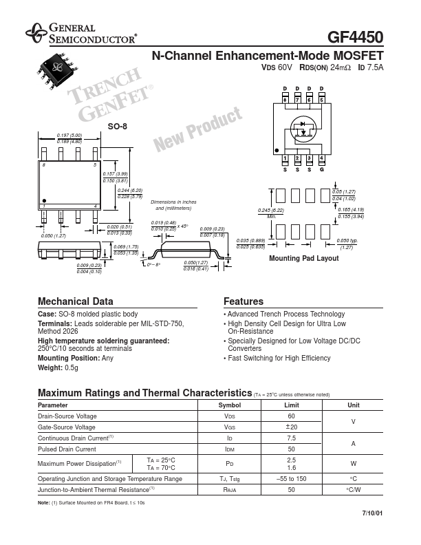
 SO-8 0.197 (5.00) 0.189 (4.80) 8 5 0.157 (3.99) 0.150 (3.81) 0.244 (6.20) 0.228 (5.79) 1...
View more extracted text
0.189 (4.80) 8 5 0.157 (3.99) 0.150 (3.81) 0.244 (6.20) 0.228 (5.79) 1 4 VDS 60V RDS(ON) 24mΩ ID 7.5A ® t c u rod P New 0.05 (1.27) 0.04 (1.02) 0.245 (6.22) Min. 0.009 (0.23) 0.007 (0.18) Dimensions in inches and (millimeters) 0.019 (0.48) x 45 ° 0.010 (0.25) 0.165 (4.19) 0.155 (3.94) 0.050 (1.27) 0.020 (0.51) 0.013 (0.33) 0.069 (1.75) 0.053 (1.35) 0.009 (0.23) 0.004 (0.10) 0.035 (0.889) 0.025 (0.635) 0 °– 8 ° 0.050(1.27) 0.016 (0.41) 0.050 typ. (1.27) Mounting Pad Layout Mechanical Data Case: SO-8 molded plastic body Terminals: Leads solderable per MIL-STD-750, Method 2026 High temperature soldering guaranteed: 250°C/10 s
More Datasheets from General Semiconductor (now Vishay)